Author Archives: Hal Martin

About Hal Martin

In my free time I like experiment with hardware and embedded systems. Here I write about personal projects and random adventures into firmware land.

HP Z420 ATX modification

Using proprietary OEM motherboards outside their intended use case is not a new subject. OEM motherboards are typically less expensive than their enthusiast counterparts on the second hand market, and they often incorporate features that the enthusiast offers lack, such as an integrated TPM or additional I/O.

The HP Z420 is a workstation based on the LGA 2011 (Sandy/Ivy Bridge-EP) socket, released in 2012. There are various forum threads around the internet discussing how to operate the motherboard with a third-party power supply and chassis, however I have not found a succinct document that outlines all the steps required to use the motherboard without HP original parts.


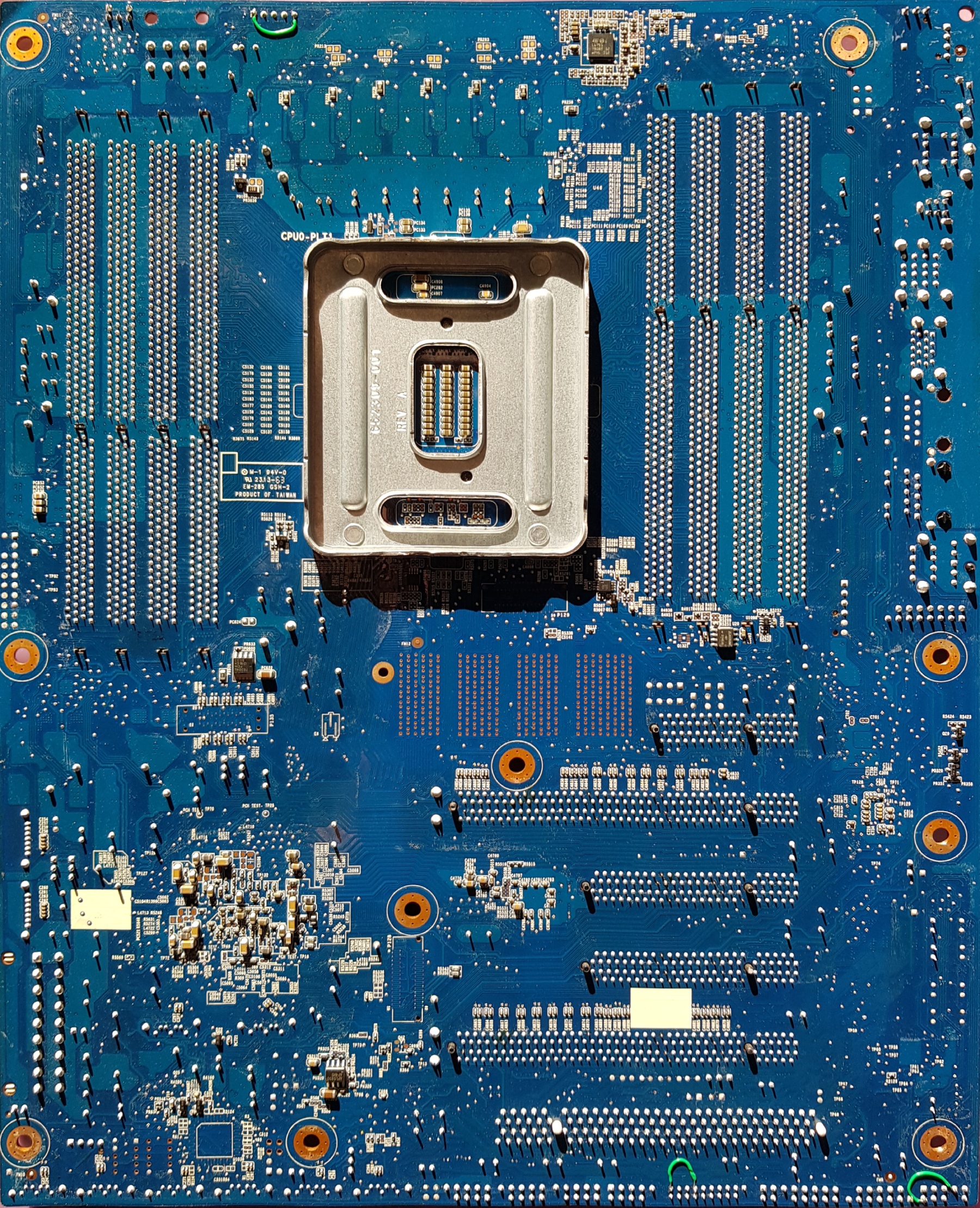
The motherboard has an 18+8pin power arrangement. The motherboard is almost entirely 12V powered, with +11VSB being the only other voltage present. The pinout of the 18 pin main power connector is as follows:

HP Z210/Z420/Z620 18 pin motherboard power pinout

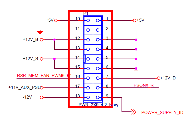
The following pins are the only pins required to power the motherboard:

Z420 PinDescriptionATX PSU pin
1, 105V output from the motherboardN/A
2-6, 11Ground3, 5, 7, 15, 17-19, 24
7, 12-1512V input10-11
8/PSON16
17+11VSB inputN/A (step-up from +5VSB)
18-12V input (not required)N/A

It is possible to inexpensively build an adapter out of a 24 pin ATX extension table and a DC buck-boost converter to step +5VSB up to +11VSB. You can also find very inexpensive adapters for sale on eBay or AliExpress which are purpose built for the Z420/Z620:

ATX to Z420/Z620 18pin adapter

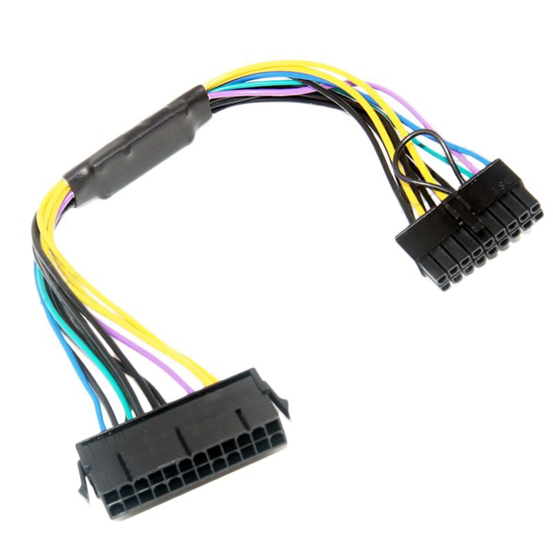
These adapters are typically around $5 and include the buck-boost circuit needed to provide +11VSB (located in the black shrink wrap mid-cable).

The 8 pin power connector on the motherboard is identical to the ATX EPS power connector. However, the EPS power is on a right angle facing the top of the motherboard, you may have clearance issues installing the motherboard into some ATX chassis.


The CPU socket backplate has extrusions which will interfere with your chassis (assuming your chassis does not have a cut-out behind the CPU for accessing the backplate without removing the motherboard). These can be removed by fatiguing the metal (repeated bending using pliers) or with a dremel.

Some other minor modifications are required to convince the motherboard that it is running inside an HP chassis.

From HP service manual (PDF)

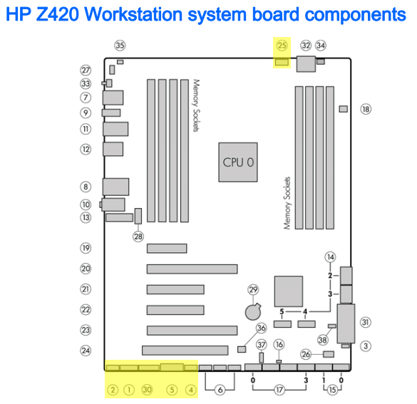
CPU fan (25): Connect pin 1 to pin 5

Front panel audio (2): Connect pin 2 (GND) to pin 4 (presence), since the pins are adjacent you can use a jumper. Connect pin 7 (sense_send) to pin 2 (GND).

Front panel IEEE1394 (1): Connect pin 11 (TPB-) to pin 12 (GND), since the pins are adjacent you can use a jumper.

Front panel LEDS (30): Connect pin 11 to Base and Collector of a 2222A NPN transistor, connect pin 12 to the 2222A Emitter.

From HP forum

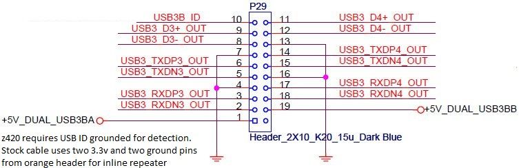
Front panel USB3.0 (5): Connect pin 10 (USB3B_ID) to GND (one of pins 4, 7, 13, 16)

From HP forum

Front panel USB2.0 (4): Connect pin 8 (GND) to pin 10 (DRAIN), since the pins are adjacent you can use a jumper.


Top view of the front-panel headers on the Z420 motherboard with modifications
HP Z420 motherboard rear showing bridged connections for CPU fan, FP-USB3.0, FP-audio

A final word on power consumption: the Z420 motherboard consumes around 40W idle (E5-2630v2), but supports ACPI suspend-to-ram (S3) and consumes around 10W when in S3. Wake-on-LAN does not work when using an ATX power supply.

Siglent SDS1000X-E license recovery

I know I am late to the “recover your license keys for your Siglent oscilloscope” party, but since I recently went through this to recover my license keys, there is a much easier approach that people don’t seem to be aware of.

There are several forum topics and blog posts on the subject of recovering license keys for the Siglent SDS1000X-E series.

Most of the methods described involve extracting the cramfs, modifying the password hash of the root user, and flashing the modified image as an update.

There is a much easier way to obtain the bandwidth and option licenses of the scope while using only official Siglent firmware images.

  1. Download the firmware 6.1.25R2
  2. Extract the archive and copy the ADS file SDS1004X_E_6.1.25R2.ADS to a FAT32 formatted USB device
  3. Follow the instructions in the 6.1.25R2 archive to “update” (downgrade) the scope firmware to 6.1.25R2
  4. Navigate to the SCPI control page of the web management interface of the scope
  5. Run the following SCPI command: SHELLCMD telnetd -l/bin/sh -p9999
  6. telnet to the scope’s IP address on port 9999
  7. Dump the memory to the USB device: cat /dev/mem > /usr/bin/siglent/usr/mass_storage/U-disk0/memdump
  8. sync and umount /usr/bin/siglent/usr/mass_storage/U-disk0
  9. On a PC, run this python script with your scope_id, serial, and the path to the memory dump
    python3 siglent_sds1000xe.py --serial SDSXXXXXXX9999 --sid 012a3456789bc012 --dump /media/usb0/memdump.bin
  10. Install the 200MHz bandwidth license through the SCPI control page using the command MCBD
  11. Install the options licenses SCPI control page using the commands:
    • LCISL AWG,<code>
    • LCISL WIFI,<code>
    • LCISL MSO,<code>
  12. Reboot the scope to apply the changes
  13. After verifying that the bandwidth and option licenses are installed, update the scope firmware to the latest release (6.1.37R8 at the time of writing)

There is no need to repack the cramfs with a new shadow file containing a known root password. Additionally, the license key extraction from memory doesn’t appear to work (or at least, did not provide valid license keys for options on my scope) so I’ve borrowed the contents of a python script from the SDS2000X thread to provide option license keys for the SDS1000X-E. The script is available here.

Note that the 6.1.25R2 firmware has the root password siglent_sds1000x_e. However the password is not required in any of the above steps.

Modifying the Sercomm AD1018 for NAND flashing

My previous work has mostly involved SPI-based flash, but more modern devices like the Meraki MR33 have only NAND storage and there are instances where it is necessary to modify the contents of NAND using hardware means (e.g. to downgrade u-boot before flashing OpenWrt).

There are a wide variety of hardware NAND flashers available on the market, however they are often expensive, proprietary, and slow. Hardware flashers like a Teensy++ 2.0 running NANDway or the NANDLite (which are both quite inexpensive options) will work for reading data, they are not at all convenient if you want to modify the data and rewrite it. Every NAND chip is unique and has its own bad blocks which you should take into consideration. The net result using these programmers is that you have a very slow workflow: you must obtain a consistent dump of the NAND through a device which often reads at only 100KB/s, modify the contents (recalculating ECC/OOB), and then write it back to the NAND.

Why bother with all of this when Linux has a very robust and fast mtd subsystem in the kernel?


Enter the Sercomm AD1018.

Sercomm AD1018

The Sercomm AD1018 is a DSL router originally produced for Vodafone España and based on the Broadcom BCM6328. There are two hardware revisions, which are the same apart from the amount of RAM: v1 has 64MB of RAM and v2 has 128MB. It can be found on eBay from Spanish sellers for less than 20€, and is supported by OpenWrt. As a bonus, you can easily modify the hardware to add SPI flash and then boot OpenWrt off of SPI.

With the operating system booted from SPI, you have a free NAND interface to do what you want. What do we want? A cheap, Linux-based NAND dumping and flashing platform!

However, there is a problem. The “NOR” OpenWrt image for the AD1018 doesn’t include support in the kernel for BRCMNAND so although there is support in the device tree for the onboard NAND, it is unusable in Linux. This makes the device significantly less useful as a NAND flashing platform.

This is easy to solve though: copy the kernel configuration for the smp target, which includes NAND, to the generic target:

cp target/linux/bcm63xx/smp/config-default target/linux/bcm63xx/generic/

You can download the binary image to flash from here.

After flashing the NOR release of LEDE as described in the installation instructions, simply flash the new NOR image with BRCMNAND support using sysupgrade:

sysupgrade -n /tmp/openwrt-21.02.1-bcm63xx-generic-sercomm_ad1018-nor-squashfs-cfe.bin

After rebooting you should now be able to access NAND flash from OpenWrt:

[    0.877092] nand: device found, Manufacturer ID: 0x92, Chip ID: 0xf1
[    0.883812] nand: Eon NAND 128MiB 3,3V 8-bit
[    0.888227] nand: 128 MiB, SLC, erase size: 128 KiB, page size: 2048, OOB size: 64
[    0.896083] bcm6368_nand 10000200.nand: detected 128MiB total, 128KiB blocks, 2KiB pages, 16B OOB, 8-bit, Hamming ECC
[    0.908376] Bad block table found at page 65472, version 0x01
[    0.915264] Bad block table found at page 65408, version 0x01
[    0.923011] 1 fixed-partitions partitions found on MTD device brcmnand.0
[    0.930026] Creating 1 MTD partitions on "brcmnand.0":
[    0.935356] 0x000000000000-0x000008000000 : "storage"

Until now, apart from installing the SPI flash, we have only addressed software issues. The kernel output above is the stock NAND which is soldered to the PCB, not exactly practical for flashing NAND from other devices.

The OpenWrt wiki suggests hand soldering a TSOP48 socket to the PCB. I am here to tell you there is a much easier method.

You can purchase TSOP48 sockets for around $5/piece from distributors (or AliExpress) however I dislike these because I still sometimes have difficulties soldering the 0.5mm pitch of TSOP48, and wrecking a TSOP48 socket while soldering gets expensive quickly. In my opinion, there is a cheaper and easier solution: use a 24 pin 0.5mm pitch FPC connector and a TSOP48 socket for a TL866II.

The TL866II TSOP48 socket can be purchased for under $4 on AliExpress. The FPC to 2.54mm breakout PCB, 24 pin FPC cable, and 24 pin 0.5mm FPC connector can all be purchased for dirt cheap (~$0.10/piece) in lots of 10+ from AliExpress. I feel this provides numerous advantages over a surface mounted TSOP48 socket:

  • FPC connectors are very inexpensive, so if you accidentally destroy it while soldering, no big loss
  • Since the TL866II TSOP48 socket is connected via FPC cables, you can easily bring it between devices while you are iterating the flash contents

Thankfully, the designers of the TL866II TSOP48 socket routed every pin. However, you should be attentive because the pinout of the TL866II TSOP48 socket is not what you might expect:

When mounting the FPC-24P 0.5mm breakout boards, note that the odd-numbered pins are always on the outer row.

All that remains is to desolder the NAND flash and solder the FPC connectors to the AD1018 PCB

Finally, after cutting a small slot the flat flex cables can be routed outside the enclosure and the TSOP48 socket can be securely mounted

Now it is possible to put the TSOP48 NAND from another device into the socket and use tools like nanddump and dd to manipulate the contents. Since it is OpenWrt, you can even mount a remote filesystem using NFS, sshfs or similar to have even more storage.


While I feel the AD1018 is a very good NAND programmer for the price, there are a few important considerations to consider when comparing the AD1018 against commercial NAND programmers:

  • You cannot hot-swap NAND (however, it boots quickly and has a physical power switch)
  • Since brcmnand is built-in to the kernel and not a module, the router won’t boot if NAND is not present
  • Linux attempts to generate a bad block table when one isn’t present, and this may take quite a long time to complete
  • The AD1018 is likely difficult to obtain outside Europe