The HP ProLiant MicroServer Gen8 was quite the impressive budget server when it was released in 2013.
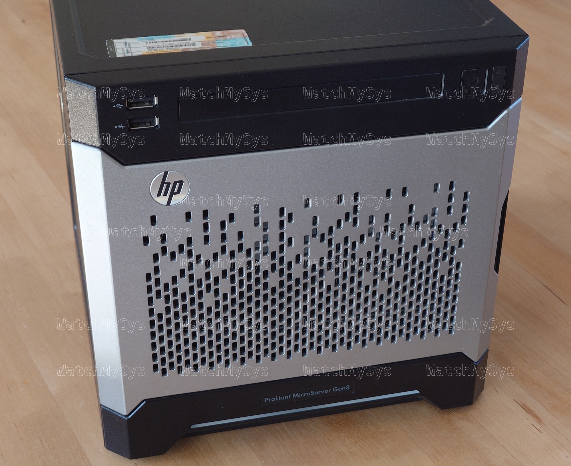
Behold the power of some CPU cores, a maximum of 16GB of DDR3 RAM, and 4 to ?? disks
Intel was dominating desktop CPUs, and a typical desktop or workstation motherboard of this era had a single PCIe 3.0 x16 slot, and then several PCIe 2.0 slots (e.g. x4 and x1). The MicroServer Gen8, due to its small size (slightly larger than ITX), was limited to only one PCIe 2.0 x16 slot. You also did not have the option to bifurcate the PCIe x16 slot, as is common in recent years.
At least, that is what everyone thought. This adventure started when I found a very interesting blog post about bifurcating the PCIe x16 slot on Intel socket 1155:
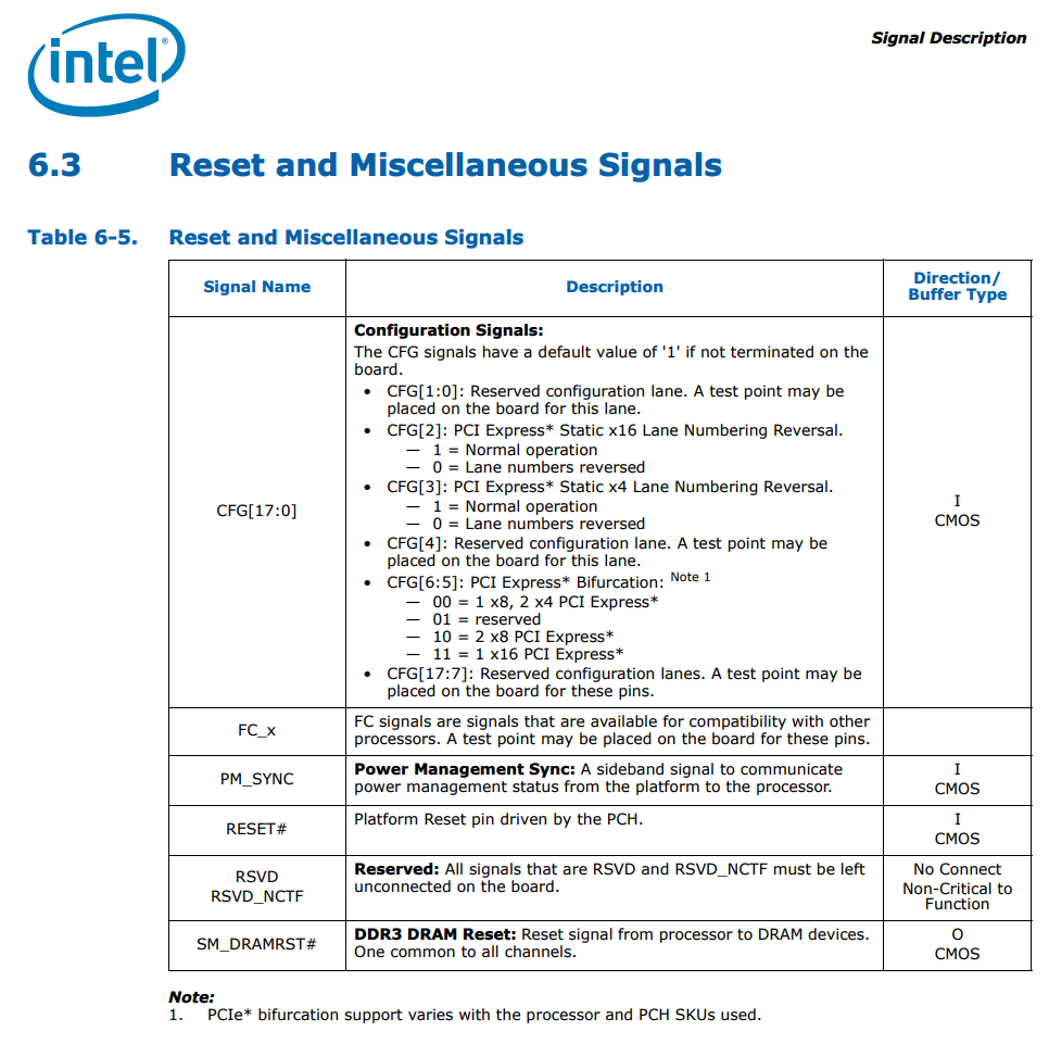
As mentioned above, I want to set 16=8+4+4, so the values of CFG[5] and CFG[6] should be both 0. So we can ground CFG[5] and CFG[6] by connecting N35M35 and L37M37. (VSS is GND, and VCC is PWR)
This information is from the Desktop 3rd Generation Intel® Core™ Processor Family, Desktop Intel® Pentium® Processor Family, and Desktop Intel® Celeron® Processor Family datasheet:
Desktop 3rd Generation Intel® Core™ Processor Family, Desktop Intel® Pentium® Processor Family, and Desktop Intel® Celeron® Processor Family
The author found that by physically bridging the pads corresponding to CFG[5] and CFG[6] they could force the PCIe x16 slot to bifurcate into x8x4x4. Since there is no official support for PCIe bifurcation on the Ivy Bridge generation, this was an interesting finding and one which I feel went largely unnoticed.
The author used silver paste, which is more permanent than what I wanted. I decided to go a more reversible route: using kapton tape and very thin strips of aluminum foil (precision cut with Fiskars scissors from a roll of baking foil).
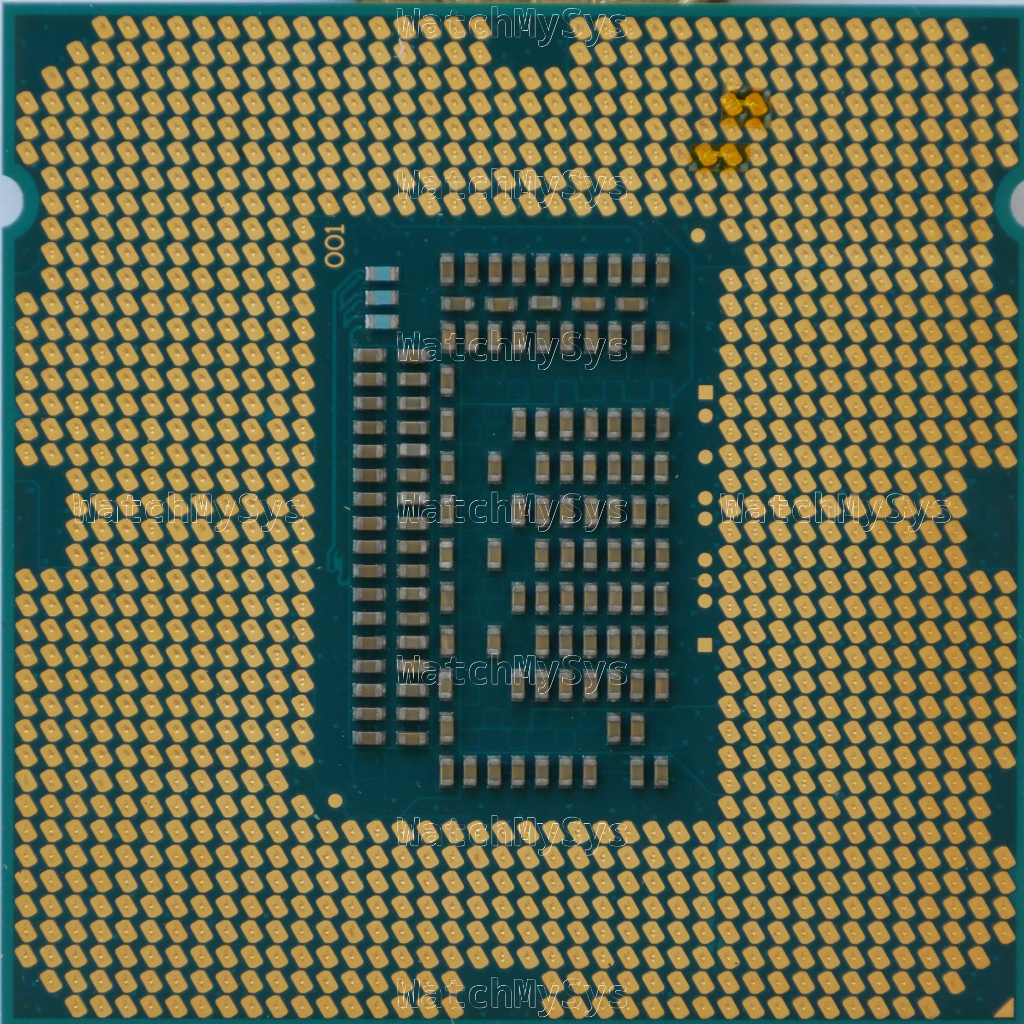
LGA1155 CPU modified for x8x4x4 bifurcation
It is important to note that by default CFG[5] and CFG[6] are pulled up to 1. Masking the pads with kapton tape is ineffective, they must be grounded to an adjacent GND pad.
WARNING: You can cause permanent damage to your CPU and motherboard by bridging incorrect pads. Always verify that the pads you have bridged are correct before installing the CPU into the socket.
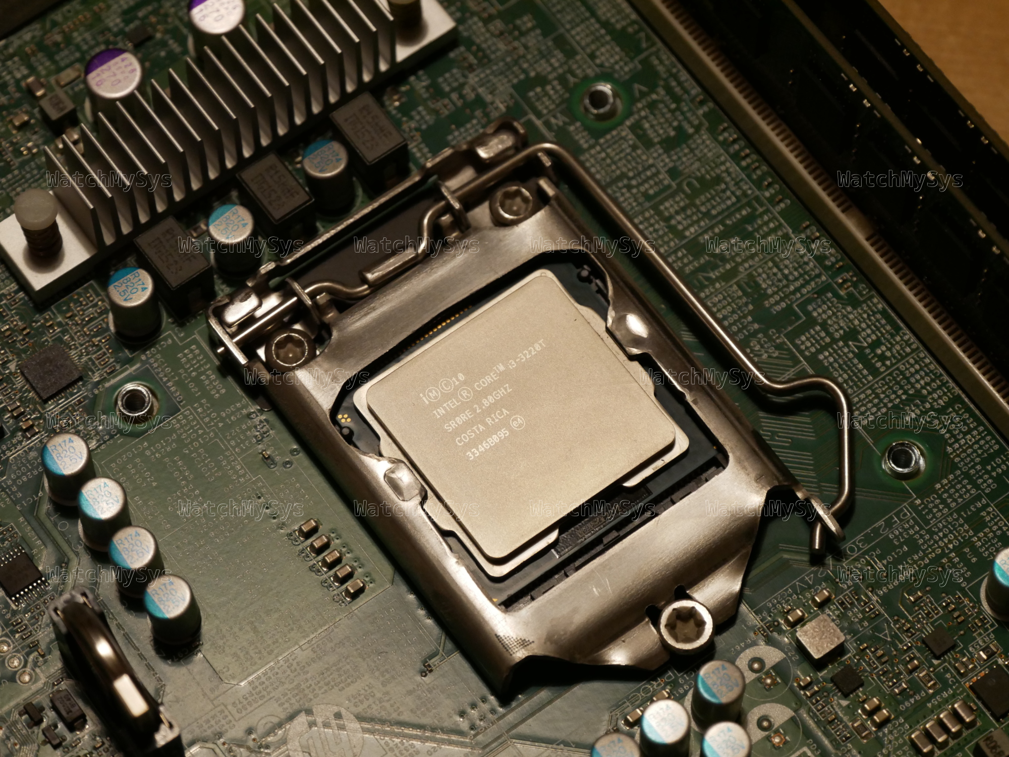
So, I obtained HP MicroServer Gen8 and got to work testing this.
Bridging both CFG[5] and CFG[6] for x8x4x4 resulted in the system hanging indefinitely during the “Processor Initialization Complete” step in POST.
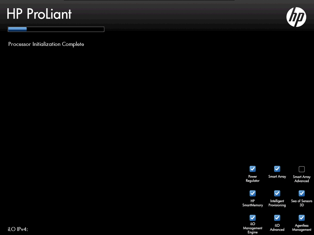
Boot stuck at “Processor Initialization Complete”
Bridging only CFG[5] to set bifurcation to x8x8 did work, and the system passed POST.
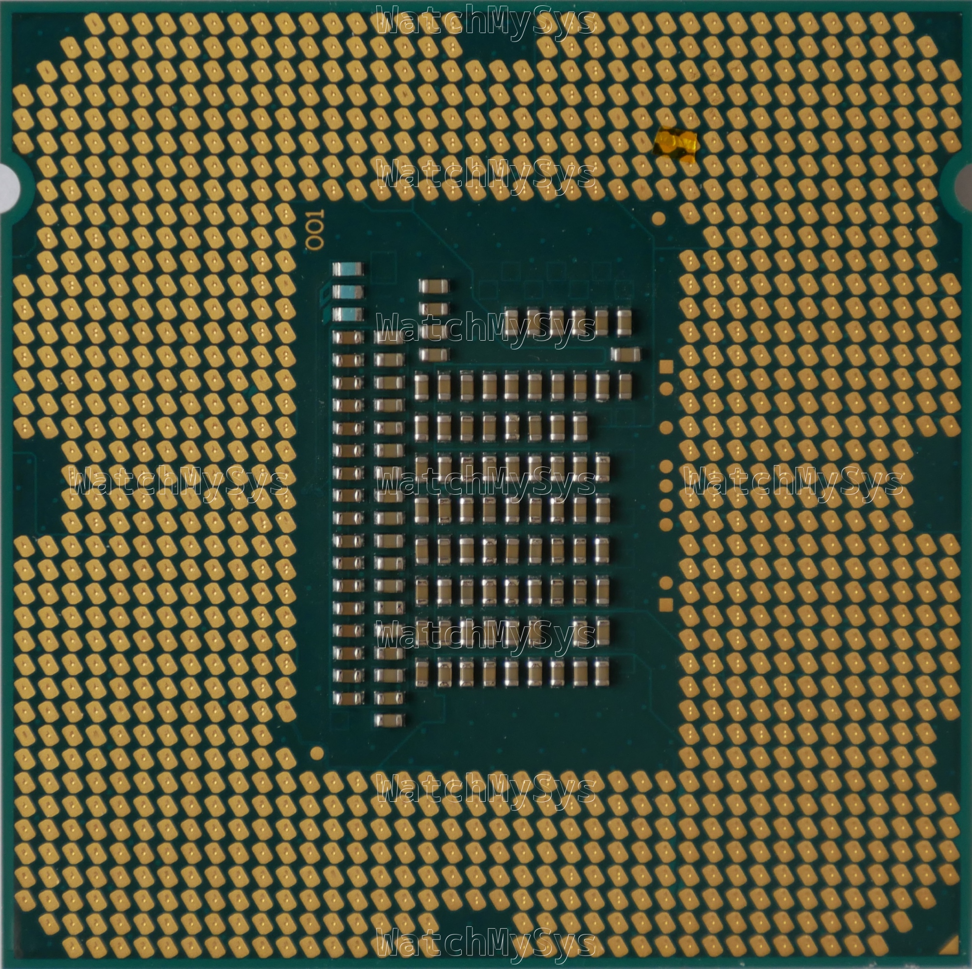
LGA1155 CPU modified for x8x8 bifurcation
With this modification, you can install two PCIe devices in the PCIe x16 slot of the MicroServer Gen8. Unfortunately due to physical constraints in the chassis, it is not possible to install a half height card on top of a half height riser (e.g. x8 and dual NVMe) but you can install a dual or quad NVMe adapter and use two PCIe x4 lanes (e.g. for an M.2 SATA controller and an M.2 2.5/5G NIC). If you do not mind PCIe cards hanging out the side, you can use a dual x8 riser like the one pictured below.
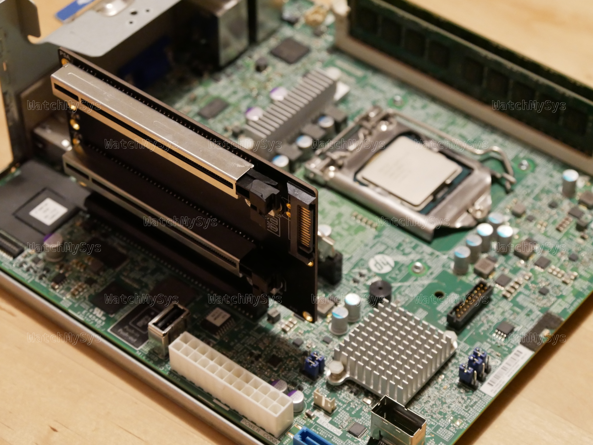
HP MicroServer Gen8 with x8x8 riser installed
Here is the lspci output of two ConnectX-3 Pro 40G network cards installed in a MicroServer Gen8:
# lspci
00:00.0 Host bridge: Intel Corporation Xeon E3-1200 v2/3rd Gen Core processor DRAM Controller (rev 09)
00:01.0 PCI bridge: Intel Corporation Xeon E3-1200 v2/3rd Gen Core processor PCI Express Root Port (rev 09)
00:01.1 PCI bridge: Intel Corporation Xeon E3-1200 v2/3rd Gen Core processor PCI Express Root Port (rev 09)
00:06.0 PCI bridge: Intel Corporation Xeon E3-1200 v2/3rd Gen Core processor PCI Express Root Port (rev 09)
00:1a.0 USB controller: Intel Corporation 6 Series/C200 Series Chipset Family USB Enhanced Host Controller #2 (rev 05)
00:1c.0 PCI bridge: Intel Corporation 6 Series/C200 Series Chipset Family PCI Express Root Port 1 (rev b5)
00:1c.4 PCI bridge: Intel Corporation 6 Series/C200 Series Chipset Family PCI Express Root Port 5 (rev b5)
00:1c.6 PCI bridge: Intel Corporation 6 Series/C200 Series Chipset Family PCI Express Root Port 7 (rev b5)
00:1c.7 PCI bridge: Intel Corporation 6 Series/C200 Series Chipset Family PCI Express Root Port 8 (rev b5)
00:1d.0 USB controller: Intel Corporation 6 Series/C200 Series Chipset Family USB Enhanced Host Controller #1 (rev 05)
00:1e.0 PCI bridge: Intel Corporation 82801 PCI Bridge (rev a5)
00:1f.0 ISA bridge: Intel Corporation C204 Chipset LPC Controller (rev 05)
00:1f.2 SATA controller: Intel Corporation 6 Series/C200 Series Chipset Family 6 port Desktop SATA AHCI Controller (rev 05)
01:00.0 System peripheral: Hewlett-Packard Company Integrated Lights-Out Standard Slave Instrumentation & System Support (rev 05)
01:00.1 VGA compatible controller: Matrox Electronics Systems Ltd. MGA G200EH
01:00.2 System peripheral: Hewlett-Packard Company Integrated Lights-Out Standard Management Processor Support and Messaging (rev 05)
01:00.4 USB controller: Hewlett-Packard Company Integrated Lights-Out Standard Virtual USB Controller (rev 02)
03:00.0 Ethernet controller: Broadcom Inc. and subsidiaries NetXtreme BCM5720 Gigabit Ethernet PCIe
03:00.1 Ethernet controller: Broadcom Inc. and subsidiaries NetXtreme BCM5720 Gigabit Ethernet PCIe
04:00.0 USB controller: Renesas Technology Corp. uPD720201 USB 3.0 Host Controller (rev 03)
07:00.0 Ethernet controller: Mellanox Technologies MT27520 Family [ConnectX-3 Pro]
0a:00.0 Ethernet controller: Mellanox Technologies MT27520 Family [ConnectX-3 Pro]
Of course the MicroServer Gen8 is very under powered and can only dream of saturating even a single 40G link.
# lspci -s 07:00.0 -vvv
07:00.0 Ethernet controller: Mellanox Technologies MT27520 Family [ConnectX-3 Pro]
        Subsystem: Hewlett-Packard Company InfiniBand FDR/Ethernet 10Gb/40Gb 2-port 544+FLR-QSFP Adapter
        Physical Slot: 1
        Control: I/O- Mem+ BusMaster+ SpecCycle- MemWINV- VGASnoop- ParErr+ Stepping- SERR- FastB2B- DisINTx+
        Status: Cap+ 66MHz- UDF- FastB2B- ParErr- DEVSEL=fast >TAbort- <TAbort- SERR- <PERR- INTx-
        Latency: 0, Cache Line Size: 64 bytes
        Interrupt: pin A routed to IRQ 16
        Region 0: Memory at fbe00000 (64-bit, non-prefetchable) [size=1M]
        Region 2: Memory at f6000000 (64-bit, prefetchable) [size=32M]
        (...)
        Capabilities: [60] Express (v2) Endpoint, IntMsgNum 0
                DevCap: MaxPayload 512 bytes, PhantFunc 0, Latency L0s <64ns, L1 unlimited
                        ExtTag- AttnBtn- AttnInd- PwrInd- RBE+ FLReset+ SlotPowerLimit 116W TEE-IO-
                DevCtl: CorrErr- NonFatalErr+ FatalErr+ UnsupReq-
                        RlxdOrd- ExtTag- PhantFunc- AuxPwr- NoSnoop- FLReset-
                        MaxPayload 256 bytes, MaxReadReq 4096 bytes
                DevSta: CorrErr+ NonFatalErr- FatalErr- UnsupReq+ AuxPwr- TransPend-
                LnkCap: Port #8, Speed 8GT/s, Width x8, ASPM L0s, Exit Latency L0s unlimited
                        ClockPM- Surprise- LLActRep- BwNot- ASPMOptComp+
                LnkCtl: ASPM Disabled; RCB 64 bytes, LnkDisable- CommClk+
                        ExtSynch- ClockPM- AutWidDis- BWInt- AutBWInt-
                LnkSta: Speed 5GT/s (downgraded), Width x8
                        TrErr- Train- SlotClk+ DLActive- BWMgmt- ABWMgmt-
                DevCap2: Completion Timeout: Range ABCD, TimeoutDis+ NROPrPrP- LTR-
                         10BitTagComp- 10BitTagReq- OBFF Not Supported, ExtFmt- EETLPPrefix-
                         EmergencyPowerReduction Not Supported, EmergencyPowerReductionInit-
                         FRS- TPHComp- ExtTPHComp-
                         AtomicOpsCap: 32bit- 64bit- 128bitCAS-
                DevCtl2: Completion Timeout: 50us to 50ms, TimeoutDis-
                         AtomicOpsCtl: ReqEn-
                         IDOReq- IDOCompl- LTR- EmergencyPowerReductionReq-
                         10BitTagReq- OBFF Disabled, EETLPPrefixBlk-
                LnkCap2: Supported Link Speeds: 2.5-8GT/s, Crosslink- Retimer- 2Retimers- DRS-
                LnkCtl2: Target Link Speed: 8GT/s, EnterCompliance- SpeedDis-
                         Transmit Margin: Normal Operating Range, EnterModifiedCompliance- ComplianceSOS-
                         Compliance Preset/De-emphasis: -6dB de-emphasis, 0dB preshoot
                LnkSta2: Current De-emphasis Level: -6dB, EqualizationComplete- EqualizationPhase1-
                         EqualizationPhase2- EqualizationPhase3- LinkEqualizationRequest-
                         Retimer- 2Retimers- CrosslinkRes: unsupported
        (...)
        Kernel driver in use: mlx4_core
        Kernel modules: mlx4_core
# lspci -s 0a:00.0 -vvv
0a:00.0 Ethernet controller: Mellanox Technologies MT27520 Family [ConnectX-3 Pro]
        Subsystem: Hewlett-Packard Company InfiniBand FDR/Ethernet 10Gb/40Gb 2-port 544+FLR-QSFP Adapter
        Control: I/O- Mem+ BusMaster+ SpecCycle- MemWINV- VGASnoop- ParErr+ Stepping- SERR- FastB2B- DisINTx+
        Status: Cap+ 66MHz- UDF- FastB2B- ParErr- DEVSEL=fast >TAbort- <TAbort- SERR- <PERR- INTx-
        Latency: 0, Cache Line Size: 64 bytes
        Interrupt: pin A routed to IRQ 16
        Region 0: Memory at fbf00000 (64-bit, non-prefetchable) [size=1M]
        Region 2: Memory at f8000000 (64-bit, prefetchable) [size=32M]
        (...)
        Capabilities: [60] Express (v2) Endpoint, IntMsgNum 0
                DevCap: MaxPayload 512 bytes, PhantFunc 0, Latency L0s <64ns, L1 unlimited
                        ExtTag- AttnBtn- AttnInd- PwrInd- RBE+ FLReset+ SlotPowerLimit 116W TEE-IO-
                DevCtl: CorrErr- NonFatalErr+ FatalErr+ UnsupReq-
                        RlxdOrd- ExtTag- PhantFunc- AuxPwr- NoSnoop- FLReset-
                        MaxPayload 128 bytes, MaxReadReq 4096 bytes
                DevSta: CorrErr- NonFatalErr- FatalErr- UnsupReq- AuxPwr- TransPend-
                LnkCap: Port #8, Speed 8GT/s, Width x8, ASPM L0s, Exit Latency L0s unlimited
                        ClockPM- Surprise- LLActRep- BwNot- ASPMOptComp+
                LnkCtl: ASPM Disabled; RCB 64 bytes, LnkDisable- CommClk+
                        ExtSynch- ClockPM- AutWidDis- BWInt- AutBWInt-
                LnkSta: Speed 5GT/s (downgraded), Width x8
                        TrErr- Train- SlotClk+ DLActive- BWMgmt- ABWMgmt-
                DevCap2: Completion Timeout: Range ABCD, TimeoutDis+ NROPrPrP- LTR-
                         10BitTagComp- 10BitTagReq- OBFF Not Supported, ExtFmt- EETLPPrefix-
                         EmergencyPowerReduction Not Supported, EmergencyPowerReductionInit-
                         FRS- TPHComp- ExtTPHComp-
                         AtomicOpsCap: 32bit- 64bit- 128bitCAS-
                DevCtl2: Completion Timeout: 50us to 50ms, TimeoutDis-
                         AtomicOpsCtl: ReqEn-
                         IDOReq- IDOCompl- LTR- EmergencyPowerReductionReq-
                         10BitTagReq- OBFF Disabled, EETLPPrefixBlk-
                LnkCap2: Supported Link Speeds: 2.5-8GT/s, Crosslink- Retimer- 2Retimers- DRS-
                LnkCtl2: Target Link Speed: 8GT/s, EnterCompliance- SpeedDis-
                         Transmit Margin: Normal Operating Range, EnterModifiedCompliance- ComplianceSOS-
                         Compliance Preset/De-emphasis: -6dB de-emphasis, 0dB preshoot
                LnkSta2: Current De-emphasis Level: -6dB, EqualizationComplete- EqualizationPhase1-
                         EqualizationPhase2- EqualizationPhase3- LinkEqualizationRequest-
                         Retimer- 2Retimers- CrosslinkRes: unsupported
        (...)
        Kernel driver in use: mlx4_core
        Kernel modules: mlx4_core
To anyone still running a MicroServer Gen8 and would like more expansion, I hope you find this information useful.