Meraki used to be friendly to open-source. Older devices and Meraki firmwares offered a root shell over UART, and it was relatively easy to flash custom firmware to the device. Later, they began locking down devices so that people could no longer repurpose the hardware. Their latest “innovations” include the use of secure boot, ostensibly to improve device security but with the side effect of making claimed and EoL devices e-waste.
“Z3 is a remote work gateway with integrated Wi-Fi, secure access to corporate and multi-cloud resources, and features that delight SD-branch cloud platform users.”
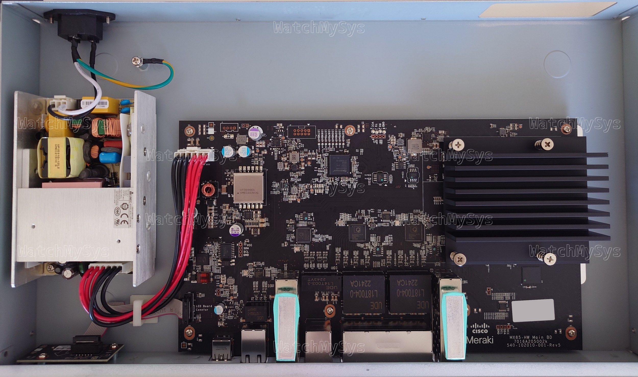
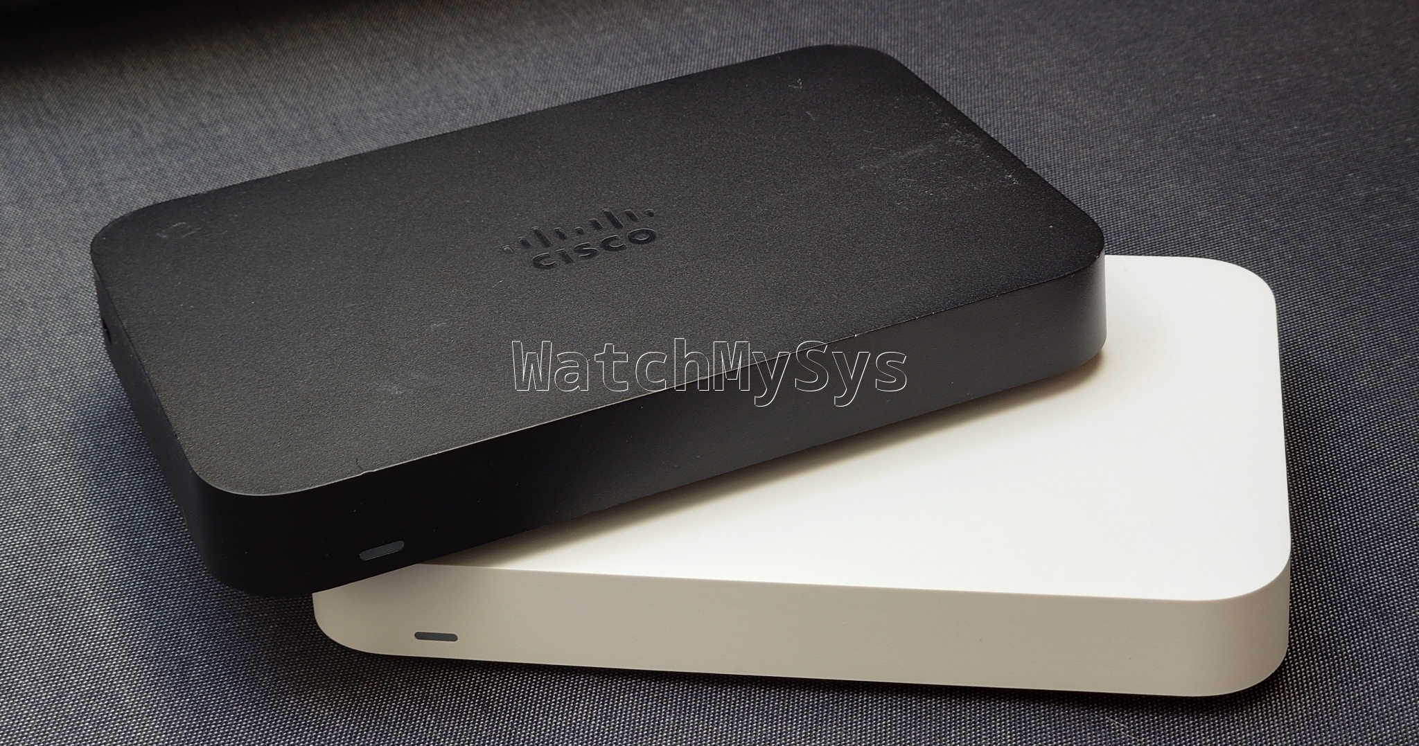
Today we are looking at the Meraki Z3 and Meraki Go GX20. Both the Z3 and GX20 ship with secure boot enabled, meaning you cannot boot an alternative firmware like OpenWrt on the devices, and they are useless if the previous owner has not “unclaimed” them in Meraki’s dashboard.
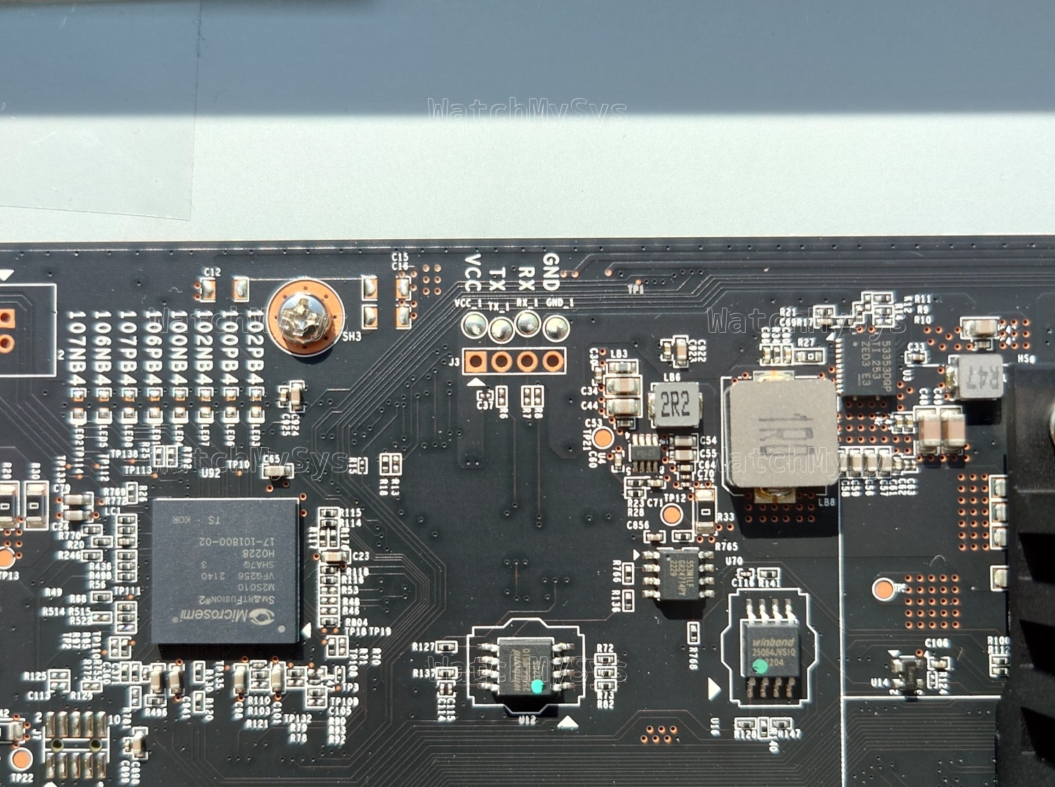
Meraki chose to use the same u-boot release for their Qualcomm IPQ40xx based devices (MR33, MR30H, Z3, Go GX20). The MR33 ships without secure boot. However, since secure boot is enabled on the Z3 and Meraki Go GX20, u-boot on those devices must be signed with a certificate matching the one burned into the QFPROM fuses, or the device will not boot. In the case of the Z3, u-boot is signed with the fuzzy-cricket attestation ca1 certificate:
California1
San Francisco
Cisco Meraki1%0#
fuzzy-cricket attestation ca1
Product Security0
170728184745Z
170827184745Z0
The boot flow on an ipq40xx device with secure boot enabled can be summarized in the following diagram (adapted from the LineageOS docs):
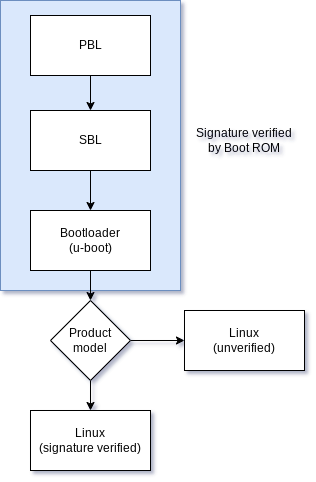
Since Meraki use the same u-boot for devices with and without secure boot, u-boot must determine at some point whether it should enforce signature verification on the payload (a Flattened Image Tree Image). That check happens here:
static int do_meraki_qca_boot(cmd_tbl_t * cmdtp, int flag, int argc, char * const argv[])
{
   /* unsupported boards */
   switch(get_meraki_product_id()) {
      case MERAKI_BOARD_STINKBUG:
      case MERAKI_BOARD_LADYBUG:
      case MERAKI_BOARD_NOISY_CRICKET:
      case MERAKI_BOARD_YOWIE:
      case MERAKI_BOARD_BIGFOOT:
      case MERAKI_BOARD_SASQUATCH:
      case MERAKI_BOARD_WOOKIE:
         return 0;
      default:
         break;
   }

   /* Check 0: check/force secure boot on */
   force_secboot();

   /* Check 1: boot diagnostic */
   run_command("run check_boot_diag_img", 0);

   /* Check 2: boot part.new if upgrading */
   do_upgrade_boot();

   /* Check 3: if node specific unlock exists, chainload u-boot */
   if (devel_crt_valid()) {
      do_chainload_uboot();
   }

   setenv("part","part.safe");
   run_command("run boot_signedpart",0);

   setenv("part","part.old");
   run_command("run boot_signedpart",0);

   run_command("reset",0);

   return 0;
}
Note that if the board is STINKBUG (MR33), LADYBUG (MR74), NOISY_CRICKET (MR30H), YOWIE (MR42), BIGFOOT (MR52), SASQUATCH (MR53), or WOOKIE (MR84) then verification of the FIT image is skipped, as these devices don’t have secure boot enabled by default.
The 2017.07 u-boot update for the MR33 is a special case, as that doesn’t actually enable secure boot, it just maliciously bricks the device if the user attempts to interrupt boot.
How this practice is permitted under the EU Unfair Commercial Practices Directive (Directive 2005/29/EC of 2005) is quite frankly a mystery to me, but perhaps someone with more legal expertise can weigh in.
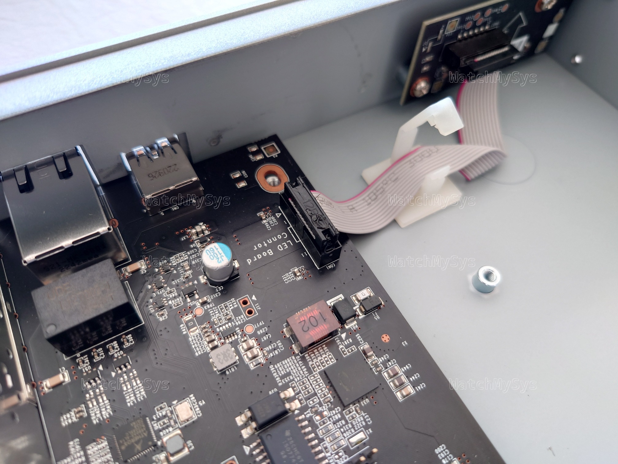
u-boot determines the device it is running on by reading the “Board major number” from an I2C EEPROM (24c64; silkscreen U32) on the PCB. Modifying the contents of the EEPROM from a device model with secure boot to a device without secure boot is enough to disable signature verification of payloads in u-boot. You can find the “board major number” byte at offset 0x49 and a backup copy at 0x1049 in the EEPROM.
Original Z3 boot output:
Format: Log Type - Time(microsec) - Message - Optional Info
Log Type: B - Since Boot(Power On Reset),  D - Delta,  S - Statistic
S - QC_IMAGE_VERSION_STRING=BOOT.BF.3.1.1-00096
S - IMAGE_VARIANT_STRING=DAACANAZA
S - OEM_IMAGE_VERSION_STRING=CRM
S - Boot Config, 0x00000025
S - Core 0 Frequency, 0 MHz
B -       261 - PBL, Start
B -      1340 - bootable_media_detect_entry, Start
B -      2615 - bootable_media_detect_success, Start
B -      2629 - elf_loader_entry, Start
B -      7204 - auth_hash_seg_entry, Start
B -   1382243 - auth_hash_seg_exit, Start
B -   1447600 - elf_segs_hash_verify_entry, Start
B -   1569288 - PBL, End
B -   1569312 - SBL1, Start
B -   1657984 - pm_device_init, Start
D -         6 - pm_device_init, Delta
B -   1659502 - boot_flash_init, Start
D -     87535 - boot_flash_init, Delta
B -   1751079 - boot_config_data_table_init, Start
D -     14006 - boot_config_data_table_init, Delta - (419 Bytes)
B -   1767784 - clock_init, Start
D -      7575 - clock_init, Delta
B -   1778758 - CDT version:2,Platform ID:8,Major ID:1,Minor ID:0,Subtype:1
B -   1782246 - sbl1_ddr_set_params, Start
B -   1787231 - cpr_init, Start
D -         2 - cpr_init, Delta
B -   1791720 - Pre_DDR_clock_init, Start
D -         5 - Pre_DDR_clock_init, Delta
D -     13140 - sbl1_ddr_set_params, Delta
B -   1804998 - pm_driver_init, Start
D -         2 - pm_driver_init, Delta
B -   1875945 - sbl1_wait_for_ddr_training, Start
D -        27 - sbl1_wait_for_ddr_training, Delta
B -   1893463 - Image Load, Start
D -   1311048 - QSEE Image Loaded, Delta - (268504 Bytes)
B -   3205010 - Image Load, Start
D -      2116 - SEC Image Loaded, Delta - (2048 Bytes)
B -   3215195 - Image Load, Start
D -   1307290 - APPSBL Image Loaded, Delta - (292616 Bytes)
B -   4522910 - QSEE Execution, Start
D -        56 - QSEE Execution, Delta
B -   4529089 - SBL1, End
D -   2961858 - SBL1, Delta
S - Flash Throughput, 1970 KB/s  (563587 Bytes,  285975 us)
S - DDR Frequency, 672 MHz


U-Boot 2017.07-RELEASE-g39cabb9bf3 (May 24 2018 - 14:07:32 -0700)

DRAM:  242 MiB
machid : 0x8010001
Product: meraki_Fuzzy_Cricket
NAND:  ONFI device found
ID = 1d80f101
Vendor = 1
Device = f1
128 MiB
Using default environment

In:    serial
Out:   serial
Err:   serial
machid: 8010001
ubi0: attaching mtd1
ubi0: scanning is finished
ubi0: attached mtd1 (name "mtd=0", size 112 MiB)
ubi0: PEB size: 131072 bytes (128 KiB), LEB size: 126976 bytes
ubi0: min./max. I/O unit sizes: 2048/2048, sub-page size 2048
ubi0: VID header offset: 2048 (aligned 2048), data offset: 4096
ubi0: good PEBs: 896, bad PEBs: 0, corrupted PEBs: 0
ubi0: user volume: 5, internal volumes: 1, max. volumes count: 128
ubi0: max/mean erase counter: 124/51, WL threshold: 4096, image sequence number: 1218587189
ubi0: available PEBs: 337, total reserved PEBs: 559, PEBs reserved for bad PEB handling: 20


Secure boot enabled.

Read 0 bytes from volume part.safe to 84000000
No size specified -> Using max size (16584704)
Valid image
## Loading kernel from FIT Image at 84000028 ...
   Using 'config@1' configuration
   Trying 'kernel@1' kernel subimage
     Description:  wired-arm-qca Kernel
     Type:         Kernel Image
     Compression:  uncompressed
     Data Start:   0x84000134
     Data Size:    1962384 Bytes = 1.9 MiB
     Architecture: ARM
     OS:           Linux
     Load Address: 0x80208000
     Entry Point:  0x80208000
     Hash algo:    sha1
     Hash value:   1a716f7999511396baa166ef3986165f40c4c1c7
   Verifying Hash Integrity ... sha1+ OK
## Loading ramdisk from FIT Image at 84000028 ...
   Using 'config@1' configuration
   Trying 'ramdisk@1' ramdisk subimage
     Description:  wired-arm-qca Ramdisk
     Type:         RAMDisk Image
     Compression:  uncompressed
     Data Start:   0x841df3b8
     Data Size:    14496712 Bytes = 13.8 MiB
     Architecture: ARM
     OS:           Linux
     Load Address: 0x82200000
     Entry Point:  0x82200000
     Hash algo:    sha1
     Hash value:   6c03ebf4feff11ed19dadcd2b6afe329d74e6671
   Verifying Hash Integrity ... sha1+ OK
   Loading ramdisk from 0x841df3b8 to 0x82200000
## Loading fdt from FIT Image at 84000028 ...
   Using 'config@1' configuration
   Trying 'fdt@1' fdt subimage
     Description:  Fuzzy Cricket Device Tree
     Type:         Flat Device Tree
     Compression:  uncompressed
     Data Start:   0x84fb2874
     Data Size:    38216 Bytes = 37.3 KiB
     Architecture: ARM
     Hash algo:    sha1
     Hash value:   25733212c52b5e5803c8fe02a64fd229f30a2ac4
   Verifying Hash Integrity ... sha1+ OK
   Loading fdt from 0x84fb2874 to 0x89000000
   Booting using the fdt blob at 0x89000000
   Loading Kernel Image ... OK
   Using Device Tree in place at 89000000, end 8900c547
Using machid 0x8010001 from environment

Starting kernel ...
After modifying the Z3 EEPROM to have the board major number of the MR33:
Format: Log Type - Time(microsec) - Message - Optional Info
Log Type: B - Since Boot(Power On Reset),  D - Delta,  S - Statistic
S - QC_IMAGE_VERSION_STRING=BOOT.BF.3.1.1-00096
S - IMAGE_VARIANT_STRING=DAACANAZA
S - OEM_IMAGE_VERSION_STRING=CRM
S - Boot Config, 0x00000025
S - Core 0 Frequency, 0 MHz
B -       261 - PBL, Start
B -      1340 - bootable_media_detect_entry, Start
B -      2615 - bootable_media_detect_success, Start
B -      2629 - elf_loader_entry, Start
B -      7204 - auth_hash_seg_entry, Start
B -   1382292 - auth_hash_seg_exit, Start
B -   1447925 - elf_segs_hash_verify_entry, Start
B -   1569633 - PBL, End
B -   1569657 - SBL1, Start
B -   1658338 - pm_device_init, Start
D -         6 - pm_device_init, Delta
B -   1659859 - boot_flash_init, Start
D -     87566 - boot_flash_init, Delta
B -   1751466 - boot_config_data_table_init, Start
D -     14002 - boot_config_data_table_init, Delta - (419 Bytes)
B -   1768163 - clock_init, Start
D -      7570 - clock_init, Delta
B -   1779133 - CDT version:2,Platform ID:8,Major ID:1,Minor ID:0,Subtype:1
B -   1782622 - sbl1_ddr_set_params, Start
B -   1787606 - cpr_init, Start
D -         2 - cpr_init, Delta
B -   1792095 - Pre_DDR_clock_init, Start
D -         5 - Pre_DDR_clock_init, Delta
D -     13141 - sbl1_ddr_set_params, Delta
B -   1805373 - pm_driver_init, Start
D -         2 - pm_driver_init, Delta
B -   1876249 - sbl1_wait_for_ddr_training, Start
D -        27 - sbl1_wait_for_ddr_training, Delta
B -   1893981 - Image Load, Start
D -   1311108 - QSEE Image Loaded, Delta - (268504 Bytes)
B -   3205588 - Image Load, Start
D -      2122 - SEC Image Loaded, Delta - (2048 Bytes)
B -   3215674 - Image Load, Start
D -   1307310 - APPSBL Image Loaded, Delta - (292616 Bytes)
B -   4523411 - QSEE Execution, Start
D -        56 - QSEE Execution, Delta
B -   4529587 - SBL1, End
D -   2962011 - SBL1, Delta
S - Flash Throughput, 1969 KB/s  (563587 Bytes,  286173 us)
S - DDR Frequency, 672 MHz


U-Boot 2017.07-RELEASE-g39cabb9bf3 (May 24 2018 - 14:07:32 -0700)

DRAM:  242 MiB
machid : 0x8010001
Product: meraki_Stinkbug
NAND:  ONFI device found
ID = 1d80f101
Vendor = 1
Device = f1
128 MiB
Using default environment

In:    serial
Out:   serial
Err:   serial
machid: 8010001
ubi0: attaching mtd1
ubi0: scanning is finished
ubi0: attached mtd1 (name "mtd=0", size 112 MiB)
ubi0: PEB size: 131072 bytes (128 KiB), LEB size: 126976 bytes
ubi0: min./max. I/O unit sizes: 2048/2048, sub-page size 2048
ubi0: VID header offset: 2048 (aligned 2048), data offset: 4096
ubi0: good PEBs: 896, bad PEBs: 0, corrupted PEBs: 0
ubi0: user volume: 5, internal volumes: 1, max. volumes count: 128
ubi0: max/mean erase counter: 124/52, WL threshold: 4096, image sequence number: 1218587189
ubi0: available PEBs: 337, total reserved PEBs: 559, PEBs reserved for bad PEB handling: 20
Read 0 bytes from volume part.safe to 84000000
No size specified -> Using max size (16584704)
Wrong Image Format for bootm command
ERROR: can't get kernel image!
Read 0 bytes from volume part.old to 84000000
No size specified -> Using max size (16547840)
Wrong Image Format for bootm command
ERROR: can't get kernel image!
resetting ...
Note the change in output, the device was previously meraki_Fuzzy_Cricket but is now identified as meraki_Stinkbug, so the EEPROM modification worked. Unfortunately, the format of the FIT images differs between secure boot and non-secure boot, so the device no longer boots the stock firmware.
The MR33 board major number was chosen as u-boot selects config@1 from the FIT image for the MR33, which is the same config index used by default for the Z3. It would be possible to select any of the device models mentioned above that don’t implement secure boot, but doing so would mean u-boot attempts to boot from a different config@ entry.
Since the Z3 and Meraki Go GX20 have secure boot enabled, we cannot replace u-boot or the device will fail to boot.
0x000000000000-0x000000100000 : "sbl1"
0x000000100000-0x000000200000 : "mibib"
0x000000200000-0x000000300000 : "bootconfig"
0x000000300000-0x000000400000 : "qsee"
0x000000400000-0x000000500000 : "qsee_alt"
0x000000500000-0x000000580000 : "cdt"
0x000000580000-0x000000600000 : "cdt_alt"
0x000000600000-0x000000680000 : "ddrparams"
0x000000700000-0x000000900000 : "u-boot"
0x000000900000-0x000000b00000 : "u-boot-backup"
0x000000b00000-0x000000b80000 : "ART"
0x000000c00000-0x000007c00000 : "ubi"
However, by modifying the device major number, the (signed) u-boot will now allow booting unsigned payloads. The easiest way to proceed is to then build our own modified u-boot as a FIT image, and put it into the ubivol part.safe. After we do this, the boot process now looks like:
Format: Log Type - Time(microsec) - Message - Optional Info
Log Type: B - Since Boot(Power On Reset),  D - Delta,  S - Statistic
S - QC_IMAGE_VERSION_STRING=BOOT.BF.3.1.1-00096
S - IMAGE_VARIANT_STRING=DAACANAZA
S - OEM_IMAGE_VERSION_STRING=CRM
S - Boot Config, 0x00000025
S - Core 0 Frequency, 0 MHz
B -       261 - PBL, Start
B -      1340 - bootable_media_detect_entry, Start
B -      2615 - bootable_media_detect_success, Start
B -      2629 - elf_loader_entry, Start
B -      7270 - auth_hash_seg_entry, Start
B -   1382352 - auth_hash_seg_exit, Start
B -   1447639 - elf_segs_hash_verify_entry, Start
B -   1569353 - PBL, End
B -   1569377 - SBL1, Start
B -   1658051 - pm_device_init, Start
D -         6 - pm_device_init, Delta
B -   1659570 - boot_flash_init, Start
D -     87594 - boot_flash_init, Delta
B -   1751205 - boot_config_data_table_init, Start
D -     14010 - boot_config_data_table_init, Delta - (419 Bytes)
B -   1767914 - clock_init, Start
D -      7572 - clock_init, Delta
B -   1778887 - CDT version:2,Platform ID:8,Major ID:1,Minor ID:0,Subtype:1
B -   1782376 - sbl1_ddr_set_params, Start
B -   1787361 - cpr_init, Start
D -         2 - cpr_init, Delta
B -   1791851 - Pre_DDR_clock_init, Start
D -         5 - Pre_DDR_clock_init, Delta
D -     13143 - sbl1_ddr_set_params, Delta
B -   1805130 - pm_driver_init, Start
D -         2 - pm_driver_init, Delta
B -   1876340 - sbl1_wait_for_ddr_training, Start
D -        27 - sbl1_wait_for_ddr_training, Delta
B -   1893870 - Image Load, Start
D -   1312117 - QSEE Image Loaded, Delta - (268504 Bytes)
B -   3206486 - Image Load, Start
D -      2118 - SEC Image Loaded, Delta - (2048 Bytes)
B -   3216578 - Image Load, Start
D -   1308369 - APPSBL Image Loaded, Delta - (292616 Bytes)
B -   4525372 - QSEE Execution, Start
D -        56 - QSEE Execution, Delta
B -   4531549 - SBL1, End
D -   2964253 - SBL1, Delta
S - Flash Throughput, 1969 KB/s  (563587 Bytes,  286154 us)
S - DDR Frequency, 672 MHz


U-Boot 2017.07-RELEASE-g39cabb9bf3 (May 24 2018 - 14:07:32 -0700)

DRAM:  242 MiB
machid : 0x8010001
Product: meraki_Stinkbug
NAND:  ONFI device found
ID = 1d80f101
Vendor = 1
Device = f1
128 MiB
Using default environment

In:    serial
Out:   serial
Err:   serial
machid: 8010001
ubi0: attaching mtd1
ubi0: scanning is finished
ubi0: attached mtd1 (name "mtd=0", size 112 MiB)
ubi0: PEB size: 131072 bytes (128 KiB), LEB size: 126976 bytes
ubi0: min./max. I/O unit sizes: 2048/2048, sub-page size 2048
ubi0: VID header offset: 2048 (aligned 2048), data offset: 4096
ubi0: good PEBs: 896, bad PEBs: 0, corrupted PEBs: 0
ubi0: user volume: 5, internal volumes: 1, max. volumes count: 128
ubi0: max/mean erase counter: 214/99, WL threshold: 4096, image sequence number: 2086049366
ubi0: available PEBs: 0, total reserved PEBs: 896, PEBs reserved for bad PEB handling: 20
Read 0 bytes from volume part.safe to 84000000
No size specified -> Using max size (507904)
## Loading kernel from FIT Image at 84000000 ...
   Using 'config@1' configuration
   Trying 'kernel-1' kernel subimage
     Description:  Kernel
     Type:         Kernel Image
     Compression:  uncompressed
     Data Start:   0x840000d0
     Data Size:    381216 Bytes = 372.3 KiB
     Architecture: ARM
     OS:           Linux
     Load Address: 0x87300000
     Entry Point:  0x87300000
     Hash algo:    sha1
     Hash value:   89c319b76738e71147631f87311fc8f31e8ac8aa
   Verifying Hash Integrity ... sha1+ OK
## Loading fdt from FIT Image at 84000000 ...
   Using 'config@1' configuration
   Trying 'fdt-1' fdt subimage
     Description:  Insect DTB
     Type:         Flat Device Tree
     Compression:  uncompressed
     Data Start:   0x8405d2d4
     Data Size:    235 Bytes = 235 Bytes
     Architecture: ARM
     Hash algo:    sha1
     Hash value:   86c47255d86f2bd6301e7772ca65b3548493875b
   Verifying Hash Integrity ... sha1+ OK
   Booting using the fdt blob at 0x8405d2d4
   Loading Kernel Image ... OK
   Using Device Tree in place at 8405d2d4, end 840603be
Using machid 0x8010001 from environment

Starting kernel ...


U-Boot 2017.07-DEVEL (Apr 01 2024 - 14:50:01 +0000)

DRAM:  242 MiB
machid : 0x8010001
Product: meraki_Stinkbug
NAND:  ONFI device found
ID = 1d80f101
Vendor = 1
Device = f1
128 MiB
Using default environment

In:    serial
Out:   serial
Err:   serial
machid: 8010001
Net:   MAC0 addr:e0:cb:bc:11:22:33
PHY ID1: 0x4d
PHY ID2: 0xd0b1
ipq40xx_ess_sw_init done
eth0
Autoboot in 5 seconds
FUZZY CRICKET #
We could proceed by putting OpenWrt directly in part.safe however if we ever had a bad flash there would be no way to recover except by manually reflashing NAND. Chain loading a u-boot build does delay booting by a few seconds, but offers a way to recover from a bad flash with just UART and tftpboot.
With the modified u-boot on flash, we can now tftpboot the OpenWrt initramfs and install it to flash with sysupgrade.
“Meraki Go offers simple networks for serious business.”
The Meraki Go GX20 uses the same PCB as the Z3, but without the WiFi radios populated (the lack of WiFi means you won’t find the GX20 in the FCC database). So, does the above technique work for the Meraki Go GX20?
U-Boot 2012.07-g03cdfe19e00f [local,local] (Aug 29 2017 - 11:59:45)

DRAM:  498 MiB
machid : 0x8010001
ERROR: Unknown board
NAND:  ONFI device found
ID = 1d80f101
Vendor = 1
Device = f1
128 MiB
Using default environment

In:    serial
Out:   serial
Err:   serial
machid: 8010001
Hit any key to stop autoboot:  0
Creating 1 MTD partitions on "nand0":
0x000000c00000-0x000007f00000 : "mtd=0"
UBI: attaching mtd1 to ubi0
UBI: physical eraseblock size:   131072 bytes (128 KiB)
UBI: logical eraseblock size:    126976 bytes
UBI: smallest flash I/O unit:    2048
UBI: VID header offset:          2048 (aligned 2048)
UBI: data offset:                4096
UBI: attached mtd1 to ubi0
UBI: MTD device name:            "mtd=0"
UBI: MTD device size:            115 MiB
UBI: number of good PEBs:        920
UBI: number of bad PEBs:         0
UBI: max. allowed volumes:       128
UBI: wear-leveling threshold:    4096
UBI: number of internal volumes: 1
UBI: number of user volumes:     7
UBI: available PEBs:             364
UBI: total number of reserved PEBs: 556
UBI: number of PEBs reserved for bad PEB handling: 9
UBI: max/mean erase counter: 2/0
Read 0 bytes from volume part.safe to 84000000
No size specified -> Using max size (3284992)
## Booting kernel from FIT Image at 84000000 ...
   Using 'config@1' configuration
   Verifying Hash Integrity ... sha384,secp384r1:wired-arm-qca-RT-SECP384R1_1-rel+ OK
   Trying 'kernel@1' kernel subimage
No, unfortunately for u-boot 2012.07 which shipped on the Meraki Go GX20 I purchased, changing the device major results in ERROR: Unknown board and we can see from the sha384,secp384r1:wired-arm-qca-RT-SECP384R1_1-rel+ OK output that signature checking is still enabled.
However, the Meraki Go GX20 is a very similar device to the Z3. Is it possible that there is another way?
Examining the u-boot region of the Meraki Go GX20 with strings reveals the following:
California1
San Francisco
Cisco Meraki1%0#
fuzzy-cricket attestation ca1
Product Security0
170728184745Z
170827184745Z0
So the u-boot binary on the Meraki Go GX20 is signed with the same signing cert as u-boot on the Z3. What if we replace u-boot on the Meraki Go GX20 with the signed u-boot from the Z3 dump?
U-Boot 2017.07-RELEASE-g39cabb9bf3 (May 24 2018 - 14:07:32 -0700)

DRAM:  242 MiB
machid : 0x8010001
Product: meraki_Stinkbug
NAND:  ONFI device found
ID = 1d80f101
Vendor = 1
Device = f1
128 MiB
Using default environment
Bingo. And since the Z3 2017.07 u-boot release contains the secure boot downgrade bug, we can exploit it on the Meraki Go GX20 as well.
I am curious to see how u-boot 2012.07 on the Meraki Go GX20 implements signature validation, since unlike u-boot 2017.07 changing the device major does not disable signature verification of the payload.
Unfortunately, this is not possible. The GPL source code for the Meraki Go GX20 was requested in December 2022 and Meraki has yet to provide the u-boot source code for the device.
The EU and other jurisdictions claim to take the right to repair and e-waste seriously, but their actions thus far have ignored the elephant in the room. Many of the devices being sold in the past 5 years come with secure boot enabled, and thus are locked to running the OEM’s software.
In the case of the Meraki prodcuts, you have purchased the device and Meraki are selling a license only for the cloud management and hardware replacement service. But, if you stop paying Meraki, buy a “claimed” second-hand device, or Meraki discontinue support for the device you now have a worthless brick.
“Cisco Meraki may find it necessary to discontinue products for a number of reasons, including product line enhancements, market demand, technology innovation, or if the product simply matures over time and needs to be replaced by something functionally richer.”
To be clear, you are not leasing the hardware, and this is not “Hardware as a Service” you have bought the device in question and own it.
There are hundreds of SMD resistors on the device’s PCB. Any one of them could be tied to a GPIO which is polled by the SoC BootROM to enable or disable secure boot. Incorporating this into the hardware design would cost nothing, and would allow consumers the choice to re-use devices that were resold without proper decommissioning, from companies that were liquidated, from devices that were recycled as e-waste, or from devices where the manufacturer has decided to “maximize shareholder value” and end support. Physically opening the device and adding or removing a component to disable secure boot does not compromise user security in any way.
Routers like the Z3 and Meraki Go GX20 may appear to the untrained eye to be highly specialized devices, but in reality they are very similar to a Raspberry Pi with additional network interfaces, e.g. they are general purpose embedded computers.
It is past time that regulators start considering the user-harmful practices of companies in enforcing secure boot on these devices with no way for consumers to exercise their rights. This anti-consumer behaviour increases costs and creates more e-waste, solely for the benefit of the bottom line of companies that are (often) not even based in the same economic area. We should not, and cannot, accept such a status quo. There is no reason for these devices to become e-waste!
Impact: Device owners with physical access to their device and the appropriate hardware flashing tools can install a custom firmware.
Could this be accomplished remotely? No, not unless it is chained with another exploit providing Remote Code Execution (RCE) on the device. Anyone with an RCE on Meraki devices would not waste it on flashing a FOSS firmware, they would use it to build a botnet.
Can Meraki patch this? Yes, see below it is trivial for them to add a check in u-boot 2017.07 whether secure boot is enabled and enforce signature verification. Patching this is left as an exercise to the reader.
Will they patch it? Meraki announced the EoL of the Z3 in March 2024. They have previously been rumoured to update u-boot to brick devices when users attempt to flash a custom firmware. It remains to be seen if they will continue this anti-consumer practice on the Z3 and Meraki Go GX20.
Responsible disclosure: Yes, this has been responsibly disclosed to you, the device owner.
2024-06: The above method has also been confirmed to bypass FIT signature verification on the Meraki Z3C.
2024-07: Meraki inadvertently addressed this vulnerability in U-Boot builds dated U-Boot 2017.07-RELEASE-gf49d105aeb-dirty (Jul 13 2020 - 11:22:51 -0700) and later when they removed support for devices without secure boot (MR33, MR30H, MR74).