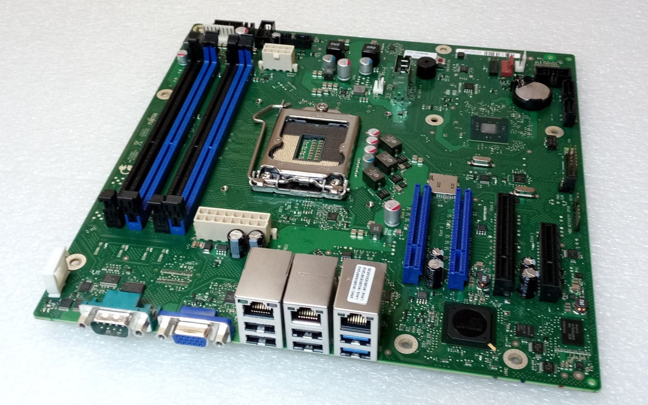
Fujitsu servers come with a remote management solution called iRMC S4 (newer models have iRMC S5). iRMC S4 and S5 are like other lights-out remote management solutions from HP (iLO) or Dell (iDRAC) which comprises a baseband management controller firmware along with other software utilities to remotely configure and manage servers. Importantly though, iRMC S4 runs Linux.
Before we get into the hardware of iRMC S4, let us examine the firmware update process. iRMC S4 follows a pretty typical BMC firmware update process: Fujitsu’s support website offers firmware downloads, and the iRMC web management interface allows you to upload the update which is then written to the inactive firmware slot.
As is common for enterprise hardware, there is no rollback protection, so you can downgrade the installed firmware to previous versions. I did not extensively test this functionality though, so there may be limits to how far you can downgrade as the firmware modifies the persistent conf partition (which is not redundant).
Running binwalk against the update file for the TX140 S2, we can immediately see that it is not encrypted:
$ binwalk FTS_TX140S2D3239iRMCKronos4FirmwareUpdatefo_TX140S20960Fsdr0344_1233853.BIN

DECIMAL       HEXADECIMAL     DESCRIPTION
--------------------------------------------------------------------------------
148820        0x24554         U-Boot version string, "U-Boot 1.1.6 (Sep 22 2015 - 17:25:45)"
150076        0x24A3C         CRC32 polynomial table, little endian
184888        0x2D238         CRC32 polynomial table, little endian
589824        0x90000         uImage header, header size: 64 bytes, header CRC: 0x2658385F, created: 2020-04-01 11:24:03, image size: 27389952 bytes, Data Address: 0x0, Entry Point: 0x0, data CRC: 0x6B45479A, OS: Linux, CPU: ARM, image type: RAMDisk Image, compression type: none, image name: ""
589888        0x90040         CramFS filesystem, little endian, size: 27389952, version 2, sorted_dirs, CRC 0x6745F599, edition 0, 15794 blocks, 4707 files
27983936      0x1AB0040       uImage header, header size: 64 bytes, header CRC: 0x27056A57, created: 2019-11-04 16:46:29, image size: 3042664 bytes, Data Address: 0x80808000, Entry Point: 0x80808000, data CRC: 0x222093D7, OS: Linux, CPU: ARM, image type: OS Kernel Image, compression type: none, image name: "Linux-3.14.17-ami"
27984000      0x1AB0080       Linux kernel ARM boot executable zImage (little-endian)
28002116      0x1AB4744       gzip compressed data, maximum compression, from Unix, last modified: 1970-01-01 00:00:00 (null date)
31129600      0x1DB0000       CramFS filesystem, little endian, size: 45056, version 2, sorted_dirs, CRC 0x52551191, edition 0, 31 blocks, 12 files
As far as I have been able to determine, here is the firmware layout of iRMC S4 on the TX140 S2:
00000000:0008ffff uboot1
00090000:01aaf040 root1 # cramfs1
01ab0040:01daffff zImage1
01db0000:01dc0000 platform1 # sdr1
01e24554:01e8ffff uboot2
01e90000:038af040 root2 # cramfs2
038b0040:03baffff zImage2
03bb0000:03bc0000 platform2 # sdr2
03c00000:03ff0000 conf
03ff0000:03ffffff fru
These correspond to the lower and higher firmware slots in iRMC S4, and ensure that the firmware you are updating is not the currently running firmware.
So, could our way into iRMC S4 be as easy as modifying the cramfs from the firmware update?
Unfortunately, no. The update is signed and the signature is checked by /usr/local/bin/flasher against an RSA-1024 public key located on the conf partition prior to overwriting:
-----BEGIN PUBLIC KEY-----
MIGfMA0GCSqGSIb3DQEBAQUAA4GNADCBiQKBgQCdgO/cGwthsFEZLuohVB5DNvU/
LolrQobsNASL4Sc+uzn8PsULIPiG0v3zhR8zCwlChmF/umVvk1gxKy5cAY0Bj3oo
cUhXwHf4t2ty+2ZY+p975Yg6YonQJSTKVPVfBlk/9PqNRj/Ih5P3zqd80YxAoKhX
i77qhLxjehHLsRSP2QIDAQAB
-----END PUBLIC KEY-----
Attempting to modify and repack cramfs results in the following output to the UART:
[1533 : 1533 INFO]VerifyImage
Signature Verification Failure
[1533 : 1533 CRITICAL][utils.c:1241]Signature verification failed
[1533 : 1533 CRITICAL][utils.c:1522]Encrypted hash of Image and the actual contents of rom.ima does not match
With our software-only modification route looking grim, it is time to move on into the realm of the evil maid.
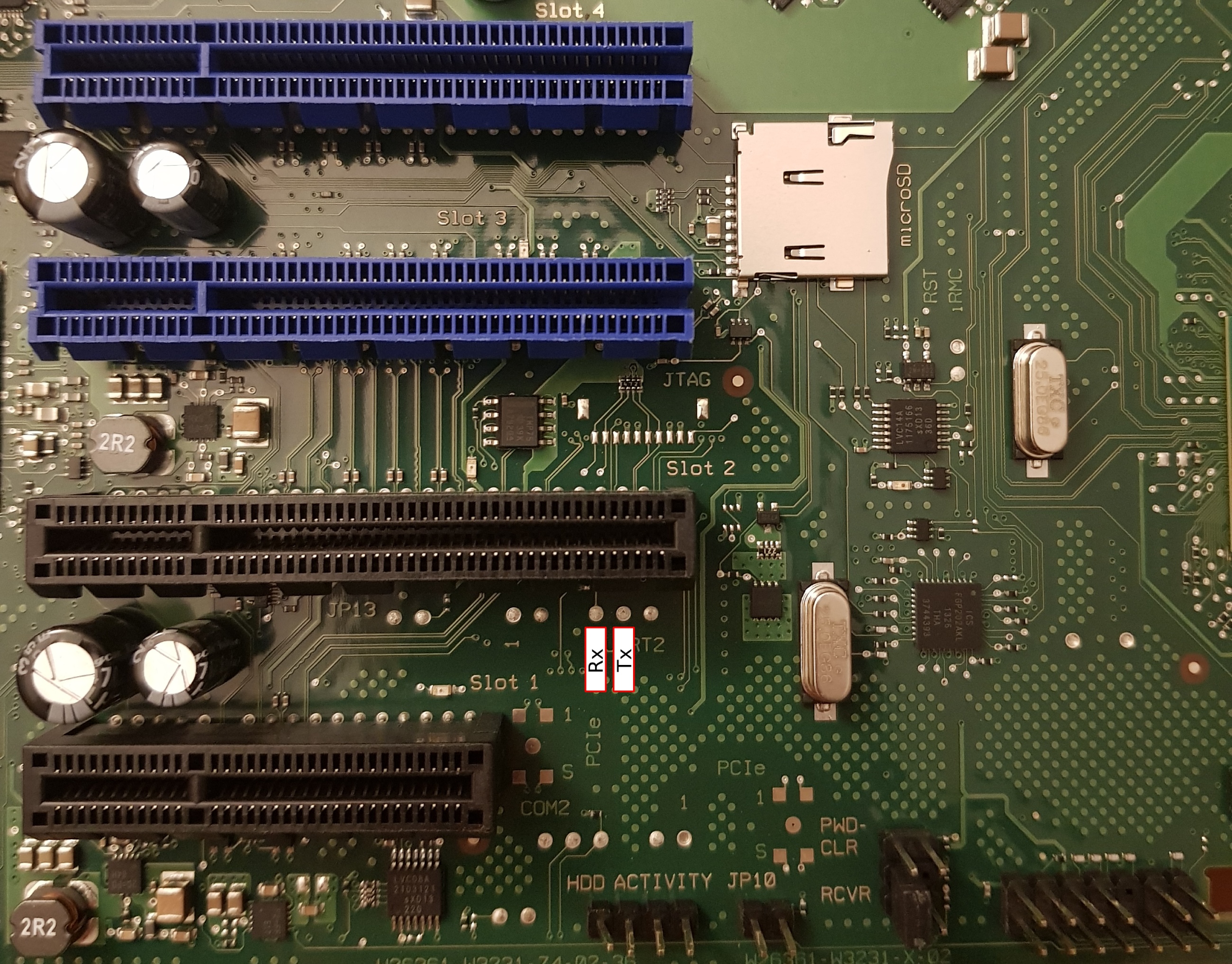
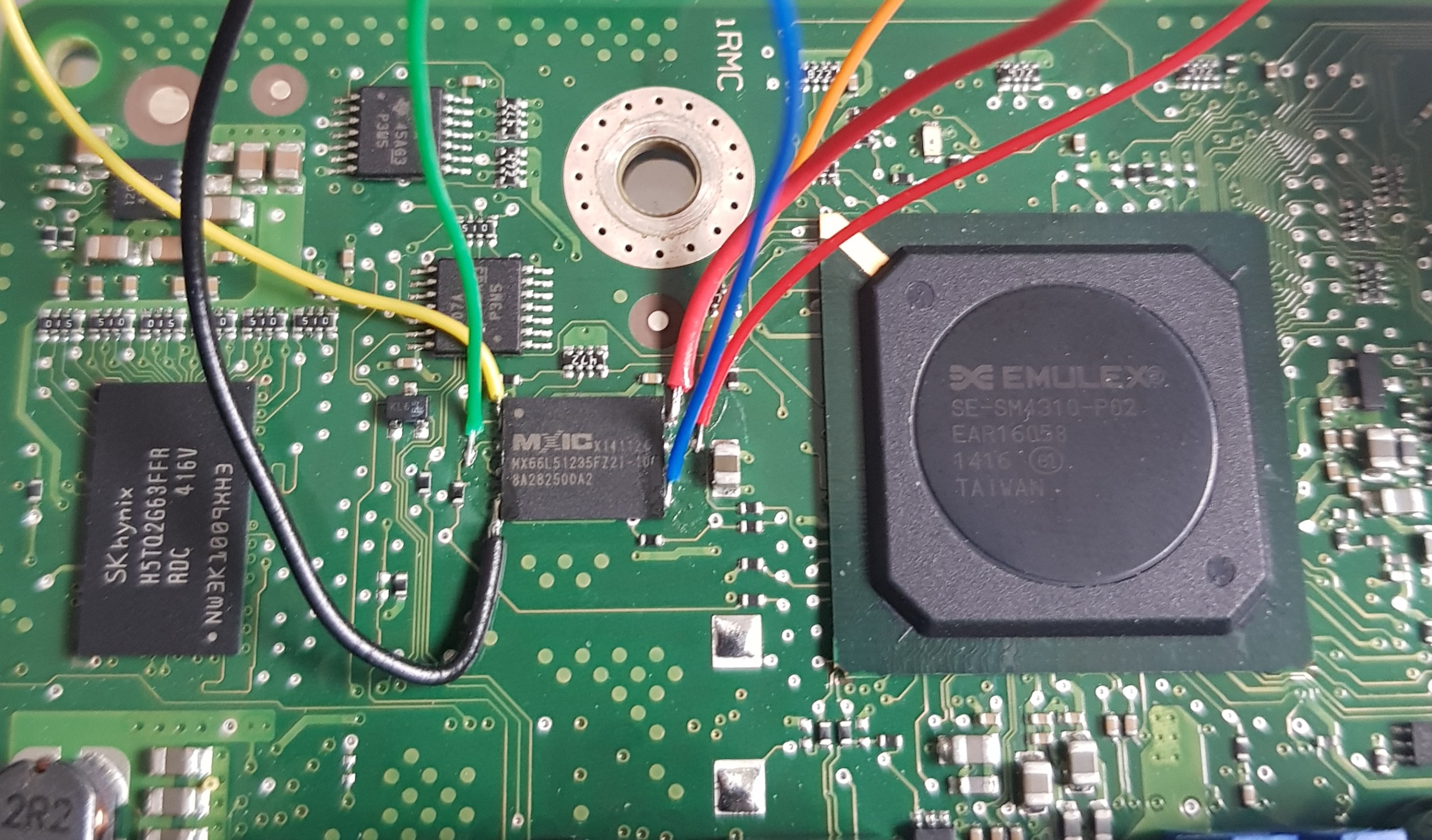
On the TX140 S2 the BMC UART (38400n8) has been routed to pads, located just below PCIe slot 2, which are easily soldered to:
To stop the default boot sequence, press Escape within 2 seconds:
U-Boot 1.1.6 (Jun 20 2013 - 09:09:05)

DRAM:  247 MB
Fast clk is set
Found SPI Chip Macronix MX66L51235F
Flash: 64 MB
Net:   pilot_eth0, pilot_eth1
Hit Esc key to stop autoboot:  0
------ Boot Options-------
        0. Normal Boot
        1. Diagnostics
        2. Remote Recovery
        3. Management Console
        4. Raw Console
Select Boot Option:
The GPL source code for iRMC S4 was requested in December 2020, and at the time of writing Fujitsu had not provided the source code. Without the source code for u-boot, it is difficult to determine if there are any routes that could lead to easy exploitation.
Getting a root console is relatively straightforward with soldering or a chip jig. If you use a jig, you will need very steady hands as flashrom requires 20-30 minutes to write and verify the 27MB cramfs region.
Lucky me, Fujitsu engineers considered physical modification of the iRMC S4 firmware out of scope, and there is no secure boot or signature verification of the cramfs on flash.
Since we can manipulate cramfs, we can bypass the stock Fujitsu shell and replace /usr/local/bin/remman with a symlink to /bin/sh and SSH as the admin user. This is not particularly useful though, as the admin user is not root sysadmin, and the busybox that Fujitsu ship is lacking the su applet, so there’s no way to easily escalate your privileges from admin to sysadmin once logged in.
~ $ id
uid=1002(admin) gid=501(ipmi) groups=501(ipmi),504(lanoem),510(serialoem),528(iRMCsettings),529(RemoteStorage),530(UserAccounts),531(VideoRedirection),532(CfgConnectionBlade),535(RemoteManager)
The uid 0 account is not called root, but rather sysadmin with the password superuser:
sysadmin:$1$A17c6z5w$5OsdHjBn1pjvN6xXKDckq0:18627:0:99999:7:::The sysadmin account is not visible in the iRMC web interface and, as far as I can tell, the password cannot be changed (unless you physically modify the contents of cramfs). I believe the account is leftover from the SDK that iRMC S4 appears to be based on.
All my attempts to login as sysadmin via SSH or uart with the default remman shell were unsuccessful, so it doesn’t appear to be a security risk out of the box.
However, once you have replaced /usr/local/bin/remman with a symlink to /bin/sh it is possible to login as the sysadmin user and enjoy root access to your iRMC S4.