Category Archives: Hardware

Meraki MS120 hardware overview

I received an innocent sounding question via GitHub, would the custom firmware I have been developing for the MS220 work on an MS120?

I am an eternal sucker for good mysteries involving hardware, so I found a seller on eBay offering an MS120-8-HW for $95 USD (plus shipping and customs to the EU). A few weeks of buyer’s remorse and waiting, and I had the MS120 in my hands.

One thing that immediately struck me about the MS120 is the material change from aluminum to steel. While I thought Meraki’s use of anodized aluminum in the MS220 series was a silly choice for the larger rack mounted models, it did make me think they were attempting to position themselves as the Apple Computer of networking products (“You pay the premium because we’re different”). Regardless of their intentions with the aluminum MS220 series, it was a precedent and it cheapens the experience to see them swap out aluminum for steel.

Let us continue, because whinging about metal choices is not bringing us closer to answering the original question.

MS120 PCB

Inside the MS120-8-HW

The MS120 is based on the Marvell Alleycat3 platform, referred to as kelpie-8 in the u-boot source and otherwise known by its marketing name “Prestera.” It is an ARMv7 core running at 400MHz with 512MB of DDR3 and 256MB of NAND flash.

The UART header is J16 at 115200n8 with the pinout:

  1. Vcc (Do not connect)
  2. Rx
  3. Tx
  4. GND

Pin 1 is closest to the SFP cage.

J17 is a mystery jumper. I have not identified its purpose yet.


There is 32Mbit (4MB) of SPI flash present, however as far as I can tell, this is connected directly to the Microsemi SmartFusion 2 and not to the Marvell ASIC. Using a hardware reader and a chip clip, I dumped the contents to examine it. Running binwalk yielded no results.

The entropy graph of the dump suggests that there are multiple copies of the same data stored, which follows Meraki’s design with the MS220 switches where there are primary and backup copies of the bootloader.

Entropy of the 32Mbit flash of the M120

Entropy graph of the 32Mbit flash in the MS120

Further inspection confirms that there are two identical copies of what I think is u-boot stored in the flash, starting at 0x301000. Each copy is approximately 420KB, which would correspond to the size of u-boot for this platform. However, the entropy is much higher than the entropy of u-boot.bin built using the Meraki GPL source, and contains only one readable string: kelpie_top

Perhaps this is the output of u-boot after running doimage to enable Secure Boot and AES-128 encryption?

The PCB traces from the winbond flash appear to go directly to the SmartFusion 2, but the u-boot UART output shows that the BootROM is booting from SPI:

BootROM 1.41
Booting from SPI flash

Is the SmartFusion 2 emulating an SPI device to the Alleycat3 after verifying the integrity of the u-boot binary in ROM?

u-boot then executes an application at memory address 0x0C100000 that prints the value of multiple “SecureBoot Registers” the strings of which do not appear anywhere in the u-boot code provided in the GPL archive:

## Starting application at 0x0C100000 ...

----Security Versions----
SecureBoot: R03.11b39af022017-07-25
SB Core: F01114R18.1680555472017-07-12
Microloader: MG0008R01.0103302017

----SecureBoot Registers----
system_invalid: 0
boot_check_count_error: 0
boot_done: 1
boot_ok: 1
boot_check_count_golden: 0
boot_check_count_upgrade: 2
boot_status_golden: 0
boot_status_upgrade: 1
first_bootloader: 1

----Upgrade----
boot_error: 0
boot_check_count_error_vc: 0
boot_check_count_error: 0
boot_timeout_vc: 0
boot_timeout: 0
boot_cs_good: 1
boot_config_error: 0
boot_version_error: 0
boot_config_error_code: 0
boot_error_code: 0
boot_cs_good: 1
boot_version_error: 0
boot1_cs_key_type: 1
boot1_cs_return_code: 0
boot1_cs_key_index: 5
boot2_cs_return_code: 0
boot2_cs_key_index: 5
boot2_cs_key_type: 1

----Other Registers----
fpga_version: 001b

Meraki do not include the build toolchain in their GPL archive. Luckily, I remembered that I have encountered this Marvell fork of u-boot before, for the Western Digital EX2100 which also uses a Marvell Armada 385 from the same family of ARMv7 CPU cores. Western Digital does include the Marvell toolchain used to compile u-boot in their GPL archive, good guy Western Digital!

To save anyone else the effort of setting up a development environment with an ancient version of GCC, I have created a Dockerfile that will handle building u-boot using the Marvell toolchain. You can find this work on GitHub.


I reached out to members of the Doozan forum who have been building Linux images for Marvell based NAS devices for many years to see if they had any more information about Secure Boot. Apparently Marvell CPUs will always kwboot before loading from other sources such as SPI or NAND:

Even if a box has secure boot in stock FW (u-boot, kernel,..), you should be able to kwboot it with a non-secure u-boot/spl binary.

I tried to kwboot the MS120 (with and without the Armada patches), but was unable to get it working. For some reason, the BootROM output is printed twice when kwboot is running, which I have not witnessed during any normal boot sequence:

$ ./kwboot -b u-boot.uart -f -t -B 115200 /dev/ttyUSB0
Sending boot message. Please reboot the target.../
BootROM 1.41
Pattern detected on UART-
BootROM 1.41
Pattern detected on UART/

uart.bin was created using tools/marvell/doimage:

$ ./doimage -T uart -D 0x0 -E 0x0 u-boot.bin u-boot.uart

Unfortunately, this investigation leaves us with more questions than answers.

  • What is the contents of the 32Mbit SPI flash?
    • Does the SmartFusion 2 only provide glue logic, or does it also protect/verify the contents of SPI flash?
  • Why won’t the Alleycat3 kwboot?
    • Is the duplicate output from BootROM when kwboot is invoked a clue?
  • What is the purpose of the header J17?
  • Why did Meraki switch from aluminum to steel?

The MS120 series is a completely different platform from the previous MS220 series, which used Vitesse ASICs with a MIPS core, 128MB of DDR2, 16MB of SPI, and 128MB of NAND flash.

The use of Secure Boot will complicate efforts to create a third-party firmware for the MS120 series. However, the more immediate issue is that kwboot does not work and there is no obvious copy of u-boot in SPI flash we can modify to alter the boot process.

Asus PN50 4700U review

The Asus PN50 is a NUC-sized mini PC based on AMD’s Renoir mobile platform. The PN50 is available in four configurations ranging from a Ryzen 3 4300U (4C/4T) to Ryzen 7 4800U (8C/16T).

I am not made of money and the 4800U commands an extreme premium for less than extreme additional performance over the 4700U (8C/8T), so I ordered the 4700U. I pre-ordered the 4700U in August for 370£ (408€) from Amazon UK (EU prices were 🤪).

Due to reasons which were never well communicated by Asus or Amazon, the release date of the product was delayed several times from early September 2020 until mid-October 2020.


tl;dr – The PN50 with the Ryzen 7 4700U offers a lot of computing power for the size and power budget, and offers a healthy amount of IO. If you are in the market for a NUC-sized PC, you would be remiss if you did not consider the PN50. The 4700U offers impressive performance, beating an i9-8950HK at one third the power.


The PN50 is sold as a barebones system, although some retailers offer it as a bundle with RAM and an SSD if you prefer overpaying for someone else installing 3 socketed components.

In the box:

  • Asus PN50
  • 19V power supply (65W for 4300/4500U, 90W for 4700/4800U)
  • IEC 60320 “mickey mouse” power cable
  • VESA mount
  • Screws for mounting the 2.5″ hard drive, M.2 SSD, and VESA mount
  • User’s guide and driver CDROM

Typical reviews are full of benchmarks (both CPU and GPU), but I want to provide my own perspective on the system so the benchmark section will be brief.

Renoir eats Intel’s mobile offers for lunch. The newest Intel system I have access to is an XPS 15 (9570) laptop with an Intel Core i9-8950HK.

Ryzen 7 4700U (Asus PN50) versus Intel Core i9-8950HK (XPS 15″ 9570)

The PN50 with Ryzen 7 4700U scores 10% higher in single-threaded performance and 12% higher in multi-core performance. The 8950HK is not the latest from Intel, but it’s still incredibly impressive that the Ryzen 7 4700U delivers superior performance at one third the power (i9-8950HK: 45W TDP; Ryzen 7 4700U: 15W TDP).


Looking at the internals of the Asus PN50, it seems that the configurable port that Asus offers on the rear is achieved by the use of a ribbon cable to a daughterboard:

DisplayPort daughterboard in the Asus PN50

On all retail units that I have seen for sale thus far, the port is configured as a full size DisplayPort. The Asus website shows DisplayPort, RS-232, VGA, and RJ-45 options under the configurable port. I don’t know if Asus ever plans to sell the FPC and daughterboards separately or if they will only be available as BTO options.

There is an FPC connector present for the secondary network (or RS-232) interface, as well as another FPC connector present for an M.2 carrier (though it isn’t clear what interface the M.2 card would use):

Unused FPC connectors for secondary LAN and M.2 card

Removing the metal guide for the bottom of the internal chassis is simple, only 4 Philips screws, and two cables (one for 2.5″ SATA connector and one for the micro SD reader):

Removing the bottom of the internal chassis is straightforward

Removing the plastic rear IO shield is also easily accomplished, as there are only 6 plastic retention clips and only 3 need to be released to remove it:

Clips to remove the plastic rear IO shield
Rear view of the PN50 with plastic IO shield removed

Unfortunately, I was unable to determine how you remove the motherboard from the chassis.


Here is the output of lspci with an NVMe SSD installed:

00:00.0 Host bridge: Advanced Micro Devices, Inc. [AMD] Renoir Root Complex
00:00.2 IOMMU: Advanced Micro Devices, Inc. [AMD] Renoir IOMMU
00:01.0 Host bridge: Advanced Micro Devices, Inc. [AMD] Renoir PCIe Dummy Host Bridge
00:01.2 PCI bridge: Advanced Micro Devices, Inc. [AMD] Renoir PCIe GPP Bridge
00:02.0 Host bridge: Advanced Micro Devices, Inc. [AMD] Renoir PCIe Dummy Host Bridge
00:02.1 PCI bridge: Advanced Micro Devices, Inc. [AMD] Renoir PCIe GPP Bridge
00:02.2 PCI bridge: Advanced Micro Devices, Inc. [AMD] Renoir PCIe GPP Bridge
00:02.3 PCI bridge: Advanced Micro Devices, Inc. [AMD] Renoir PCIe GPP Bridge
00:08.0 Host bridge: Advanced Micro Devices, Inc. [AMD] Renoir PCIe Dummy Host Bridge
00:08.1 PCI bridge: Advanced Micro Devices, Inc. [AMD] Renoir Internal PCIe GPP Bridge to Bus
00:08.2 PCI bridge: Advanced Micro Devices, Inc. [AMD] Renoir Internal PCIe GPP Bridge to Bus
00:14.0 SMBus: Advanced Micro Devices, Inc. [AMD] FCH SMBus Controller (rev 51)
00:14.3 ISA bridge: Advanced Micro Devices, Inc. [AMD] FCH LPC Bridge (rev 51)
00:18.0 Host bridge: Advanced Micro Devices, Inc. [AMD] Renoir Device 24: Function 0
00:18.1 Host bridge: Advanced Micro Devices, Inc. [AMD] Renoir Device 24: Function 1
00:18.2 Host bridge: Advanced Micro Devices, Inc. [AMD] Renoir Device 24: Function 2
00:18.3 Host bridge: Advanced Micro Devices, Inc. [AMD] Renoir Device 24: Function 3
00:18.4 Host bridge: Advanced Micro Devices, Inc. [AMD] Renoir Device 24: Function 4
00:18.5 Host bridge: Advanced Micro Devices, Inc. [AMD] Renoir Device 24: Function 5
00:18.6 Host bridge: Advanced Micro Devices, Inc. [AMD] Renoir Device 24: Function 6
00:18.7 Host bridge: Advanced Micro Devices, Inc. [AMD] Renoir Device 24: Function 7
01:00.0 USB controller: ASMedia Technology Inc. ASM1042A USB 3.0 Host Controller
02:00.0 Ethernet controller: Realtek Semiconductor Co., Ltd. RTL8111/8168/8411 PCI Express Gigabit Ethernet Controller (rev 0e)
02:00.1 Serial controller: Realtek Semiconductor Co., Ltd. Device 816a (rev 0e)
02:00.2 Serial controller: Realtek Semiconductor Co., Ltd. Device 816b (rev 0e)
02:00.3 IPMI Interface: Realtek Semiconductor Co., Ltd. Device 816c (rev 0e)
02:00.4 USB controller: Realtek Semiconductor Co., Ltd. Device 816d (rev 0e)
03:00.0 Network controller: Intel Corporation Wi-Fi 6 AX200 (rev 1a)
04:00.0 Non-Volatile memory controller: Samsung Electronics Co Ltd NVMe SSD Controller SM981/PM981/PM983
05:00.0 VGA compatible controller: Advanced Micro Devices, Inc. [AMD/ATI] Renoir (rev c2)
05:00.1 Audio device: Advanced Micro Devices, Inc. [AMD/ATI] Device 1637
05:00.2 Encryption controller: Advanced Micro Devices, Inc. [AMD] Family 17h (Models 10h-1fh) Platform Security Processor
05:00.3 USB controller: Advanced Micro Devices, Inc. [AMD] Renoir USB 3.1
05:00.4 USB controller: Advanced Micro Devices, Inc. [AMD] Renoir USB 3.1
05:00.5 Multimedia controller: Advanced Micro Devices, Inc. [AMD] Raven/Raven2/FireFlight/Renoir Audio Processor (rev 01)
05:00.6 Audio device: Advanced Micro Devices, Inc. [AMD] Family 17h (Models 10h-1fh) HD Audio Controller
05:00.7 Signal processing controller: Advanced Micro Devices, Inc. [AMD] Raven/Raven2/Renoir Sensor Fusion Hub
06:00.0 SATA controller: Advanced Micro Devices, Inc. [AMD] FCH SATA Controller [AHCI mode] (rev 81)
06:00.1 SATA controller: Advanced Micro Devices, Inc. [AMD] FCH SATA Controller [AHCI mode] (rev 81)

Here is the output of lsusb:

Bus 006 Device 001: ID 1d6b:0003 Linux Foundation 3.0 root hub
Bus 005 Device 003: ID 8087:0029 Intel Corp. 
Bus 005 Device 001: ID 1d6b:0002 Linux Foundation 2.0 root hub
Bus 004 Device 001: ID 1d6b:0003 Linux Foundation 3.0 root hub
Bus 003 Device 003: ID 0bda:0129 Realtek Semiconductor Corp. RTS5129 Card Reader Controller
Bus 003 Device 001: ID 1d6b:0002 Linux Foundation 2.0 root hub
Bus 002 Device 001: ID 1d6b:0003 Linux Foundation 3.0 root hub
Bus 001 Device 001: ID 1d6b:0002 Linux Foundation 2.0 root hub

Unfortunately the micro SDXC card reader is only connected via USB 2.0, and the maximum read speed I was able to obtain using a UHS-1 class card was 41MB/s.

This is disappointing as UHS SD cards are frequently capable of read speeds in excess of 100MB/s and Asus appears to have cost-optimized the SDXC card reader here by going with an older USB2.0 design.


I will give a brief overview of the BIOS, but suffice to say it’s pretty basic with no advanced functionality. But first, the pretty Asus splash screen:

Much incredible, so Renoir

The Main summary is quite basic, and seems to have a bug where the M.2 SSD is shown as Not Present even when installed. The bug is present in both 0409 and 0416 releases.

Summary screen of Asus PN50 0416 BIOS

Despite the Main page stating Not Present, an installed NVMe device is visible under Advanced > NVMe Configuration

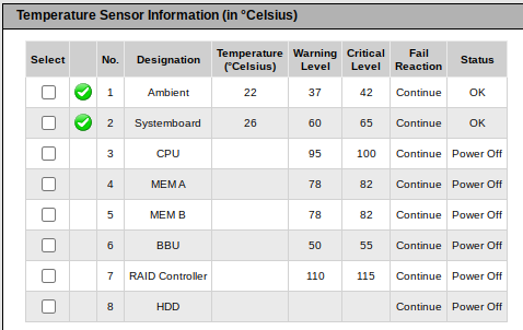
The Monitor view offers a summary of system temperatures, CPU Vcore, and fan speed. You can select the fan profile as well.

NVMe temperature is present here ¯\_(ツ)_/¯

The included EzFlash utility makes updating firmware easy, simply extract the ZIP archive containing the firmware update and put the CAP file on a FAT formatted USB device.

EzFlash: Select the update file from your USB device
Updating the firmware requires a few minutes but is otherwise painless

There seems to be a bug where you are prompted to save settings before entering the utility, and selecting No prevents you from entering EzFlash.

MCTP Configuration, DASH Configuration, and Serial Port Console Redirection are all options added in BIOS 0416 that were not present in BIOS 0409.

Advanced menu of BIOS 0416

Thus far, it seems there is no option to select a temporary boot device from the main splash screen, you must first enter BIOS and then navigate to the Boot menu. It would be nice if Asus added the option to select a temporary boot device to the splash screen in a future release.

BIOS boot menu

I had no issues with 64GB of Mushkin RAM running at 3200MHz on BIOS 0409 or BIOS 0416. The PN50 ran 4 passes of Memtest86 (BIOS 0409) without any errors.

Sadly Asus offers no option to set the cTDP at 15W or 25W. From what I’ve read, the cTDP should be set to 15W in the PN50, though I am not sure how to verify this is actually the case. It would be nice if Asus offered the option to set the cTDP at 15W or 25W, though perhaps their thermal design would not accommodate that.


I have only had my PN50 for about a week, but initial impressions are quite good. It is not overly loud and performance is quite frankly amazing for the 15W TDP.

I am really excited to use the PN50 to accelerate the time consuming tasks I have now, such as buildroot make clean && make. For someone who has been using a Xeon E3-1220v3 and Xeon E5-2620v2 for compiling, the Ryzen 7 4700U is stupidly fast and sips power. It even embarrasses the Intel i9-8950HK in the XPS 15, which is a top-spec laptop from just 2 years ago.

I am excited and cannot wait to see what Cezanne brings in 2021. Hopefully Asus see fit to update their mini PC offering for future AMD platforms.

Modifying the Cisco Meraki MS220-8P firmware

Following the analysis done by Leo Leung of the Cisco Meraki MS220-8P boot process, I wanted to share more information I’ve uncovered about the firmware source code, layout, and modification.

Cisco were not very forthcoming with the source code, and initially tried to claim that because the product was past the End of Sale, they were under no obligation to provide the source code. I am not a lawyer, but my understanding is that this claim is in violation of GPLv2 Section 3b, which states the the vendor must make the source code available for at least 3 years after the last distribution:

Accompany it with a written offer, valid for at least three years, to give any third party, for a charge no more than your cost of physically performing source distribution, a complete machine-readable copy of the corresponding source code, to be distributed under the terms of Sections 1 and 2 above on a medium customarily used for software interchange

https://opensource.org/licenses/gpl-2.0.php

I am extremely disappointed to see that Cisco is still not forthcoming with GPL source code. They have little to gain by being so difficult, and it is very disappointing to see them claiming they aren’t under obligation to provide the source code due to the product being discontinued.

To save anyone else the trouble of dragging the source code for Meraki Vitesse based switches (MS22, MS42, MS220, MS320) out of Cisco, I have mirrored the source code into 2 repositories on GitHub:

  • Stage 1 (NOR bootloader, kernel 3.18.122, includes RedBoot LinuxLoader)
  • Stage 2 (NAND firmware, kernel 3.18.123)

Please note: the kernel modules used to control the switch ASIC (vtss_core, merakiclick) are not included in the above source code. If you ever plan to build your own kernel and want to use the switch, you will need to extract the kernel modules corresponding to the above kernel versions from your switch.


My initial attempts to modify the firmware followed Leo’s instructions to disassemble the mtd region boot1. I was perplexed by the contents of the boot1-patched-post data that Leo’s script extracted from the image. The data in this region has an extremely high entropy:

The data is quite large too, approximately 200KB or 5% of the boot1 region. That’s a lot of space to give up on an embedded system for no apparent reason!

I decided to zero out the contents of this boot1-patched-post section and see what effect it would have on the boot process of the switch. The result was a kernel panic, cannot open initrd:

[    2.537000] devtmpfs: error mounting -2
[    2.541000] Warning: unable to open an initial console.
[    2.548000] VFS: Cannot open root device "(null)" or unknown-block(0,0): error -2
[    2.556000] Please append a correct "root=" boot option; here are the available partitions:
[    2.564000] 1f00          131072 mtdblock0  (driver?)
...
[    2.674000] 1f15            2670 mtdblock21  (driver?)
[    2.679000] mkp_lg: VFS: Unable to mount root fs on unknown-block(0,0)
[    2.679000] Kernel panic - not syncing: VFS: Unable to mount root fs on unknown-block(0,0)

So the kernel can no longer find the initramfs, even though the XZ archive is still present in the region. This got me thinking that the region must contain information the kernel uses to extract the XZ compressed initrd.

The build instructions I received from Meraki with the source code stated:

To build OpenWRT firmware:

cd meraki-firmware/openwrt
cp config-elemental-3.18 .config
make oldconfig
make -j1 BOARD=elemental-3.18 OPENWRT_EXTRA_BOARD_SUFFIX=_3.18


To build Linux-3.18 kernel:

cd meraki-firmware/linux-3.18
cp ../openwrt/target/linux/elemental-3.18/config .config
make CROSS_COMPILE=../openwrt/staging_dir_mipsel_nofpu_3.18/bin/mipsel-linux-musl- ARCH=mips oldconfig

make CROSS_COMPILE=../openwrt/staging_dir_mipsel_nofpu_3.18/bin/mipsel-linux-musl- ARCH=mips prepare

touch rootlist
make CROSS_COMPILE=../openwrt/staging_dir_mipsel_nofpu_3.18/bin/mipsel-linux-musl- ARCH=mips vmlinux

After following these instructions and ending up with a vmlinux that was far too big to fit into the flash region, I figured out how to build the kernel such that it fits into the boot region. This also clarified what the contents of boot1-patched-post from Leo’s extraction script contains.

To start, if you are building the 3.18.122 kernel for the SPI flash (first stage boot, before kexec) you absolutely need a rootlist file. For the stock Meraki firmware, I have re-created the contents of the rootlist file:

file /bootsh ramdisk/bootsh 755 0 0
slink /init bootsh 777 0 0
file /kexec ramdisk/kexec 755 0 0
file /MERAKI_BUILD ramdisk/MERAKI_BUILD 755 0 0
dir /bootroot 755 0 0
dir /dev 755 0 0
slink /lib bootroot/lib 777 0 0
slink /etc/ bootroot/etc 777 0 0
slink /usr bootroot/usr 777 0 0
slink /sbin bootroot/sbin 777 0 0
slink /bin bootroot/bin 777 0 0

The Meraki provided instructions produce an ELF vmlinux, which is not what at all what the switch is booting. You must use objcopy to strip vmlinux before you can get it to what the switch expects in the firmware:

mipsel-linux-musl-objcopy -O binary -S vmlinux vmlinux.bin

By following the above steps, building the kernel with the above rootlist file contents and stripping vmlinux with objcopy, vmlinux.bin is the data that goes into the boot1 region immediately after the 32 byte header. Pad the header + vmlinux.bin with zeros to ensure it is 3932160 bytes total.

Aside: You’re probably not interested in including the same files in your ramdisk as the stock Meraki firmware. Unless you have modified the NAND image to spawn a console and kill their management daemons, you’ll have the same end result as the stock firmware. However, it is a useful test to ensure that you can build and boot the kernel yourself:

Linux version 3.18.122-meraki-elemental (hmartin@alp) (gcc version 5.4.0 (GCC) ) #4 Sun Mar 1 14:44:24 UTC 2020

The meraki_stock branch of the 3.18.122 repository includes the defconfig and rootlist file you need to build the 3.18.122 kernel.


Now onto more useful matters, modifying the bootloader. I grew tired of having CRC errors when testing my changes, so I patched the CRC check out of the bootloader. Later on, I decided I wanted to try booting 3.18.123 directly from NOR, except the stripped vmlinux is nearly 5MB, too large. So I patched out the boundary check in the bootloader. You can find both versions of the bootloader (without CRC and without CRC/boundary check) in the 3.18.122 repository on GitHub.

Meraki appears to supply a common firmware for all their Vitesse based switches. The MS220-8P is based on the luton26 ASIC, while the larger switches (MS22, MS42, MS220-24/48, and MS320-24/48) appear to be based on the Jaguar-1 ASIC. Since you don’t need the kernel modules for other models in the firmware, you can delete them (and other unnecessary Meraki daemons) and fit the entire firmware in roughly 8MB using XZ compressed squashfs.

With this combination, you can boot Linux 3.18.123 from NOR, with a squashfs on NOR:

[    0.000000] Kernel command line:  console=ttyS0,115200 mtdparts=m25p80:0x40000(loader1),0x4c0000(boot1),0x800000(bootubi),0x300000(jffs2) root=/dev/mtdblock3 rootfstype=squashfs ubi.mtd=gen_nand.0 mem=0x7FF0000 ramoops.mem_address=0x7FF0000 ramoops.mem_size=0x10000 ramoops.block_size=0x10000

Since the kernel version matches the modules shipped by Meraki in their firmware, you can load the modules required to manage the ASIC:

# lsmod
vc_click 251569 0 - Live 0xc35eb000 (PO)                                                                                                                                                   
elts_meraki 4132849 1 vc_click, Live 0xc30ab000 (PO)                                                                                                                                       
merakiclick 1587774 2 vc_click,elts_meraki, Live 0xc2854000 (O)                                                                                                                            
proclikefs 5189 2 merakiclick, Live 0xc007b000 (O)                                                                                                                                         
vtss_core 663855 1 vc_click, Live 0xc13f0000 (PO)

This approach is not without its own problems. The Meraki firmware expects / to be mounted rw, something that isn’t possible with squashfs.

In summary, with the following components you can boot directly from NOR, without touching NAND at all:

Please understand that I have not solved all the issues with this approach, and above resources are intended as a guide to encourage future development. To illustrate, here is a flashable image (see here) for your MS220-8P that illustrates booting entirely from NOR. Although I would like to caution you that this is a proof of concept, not a functional firmware. If you have any improvements please submit your pull request the meraki-builder repository!

The above information is the product of months of reverse engineering, development, and testing on an MS220-8P. It is my hope that by providing the GPL archive, my modifications, build scripts, and documentation that others will find a more elegant way to run the firmware entirely from NOR, which would significantly decrease the complexity to running a custom firmware on the MS220-8P.

That’s all for now. I will continue working on this project in the background and may have more updates in the future.