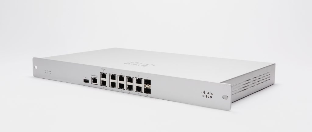
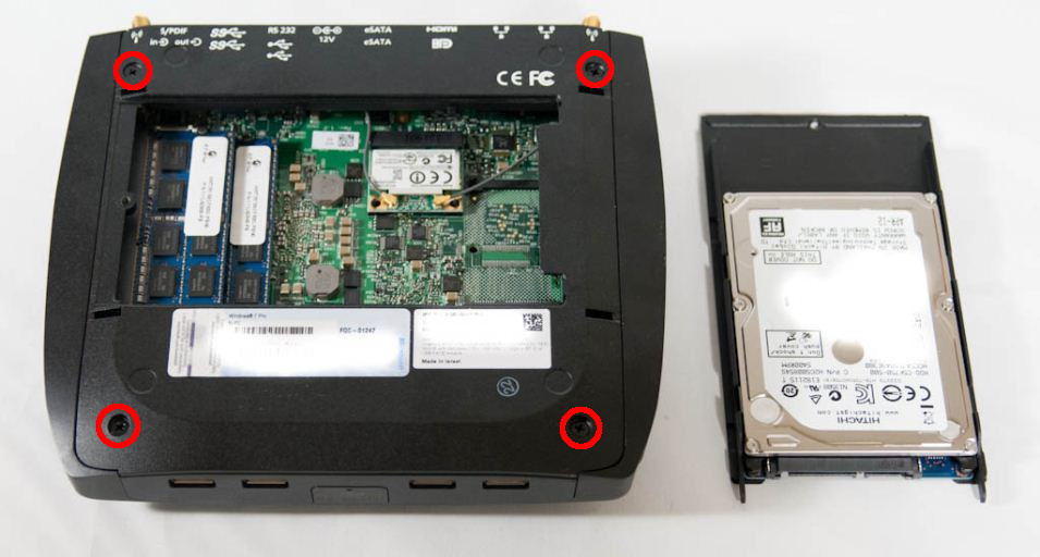
The Meraki MS350 (MS350-24 and MS350-48) series switches offer 24 or 48 ports of Gigabit Ethernet. The MS350-24X offers 16 ports of Gigabit Ethernet, and 8 ports of multi-Gigabit (1/2.5/5/10G) Ethernet. All models have four SFP/SFP+ uplink ports, a dedicated remote management port, and stacking capabilities via QSFP. Today we will be looking at the MS350-48 and MS350-24X models specifically.
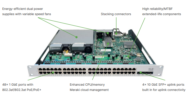
MS350-48LP from Meraki’s datasheet
Here is a quick summary of the MS350 specs:
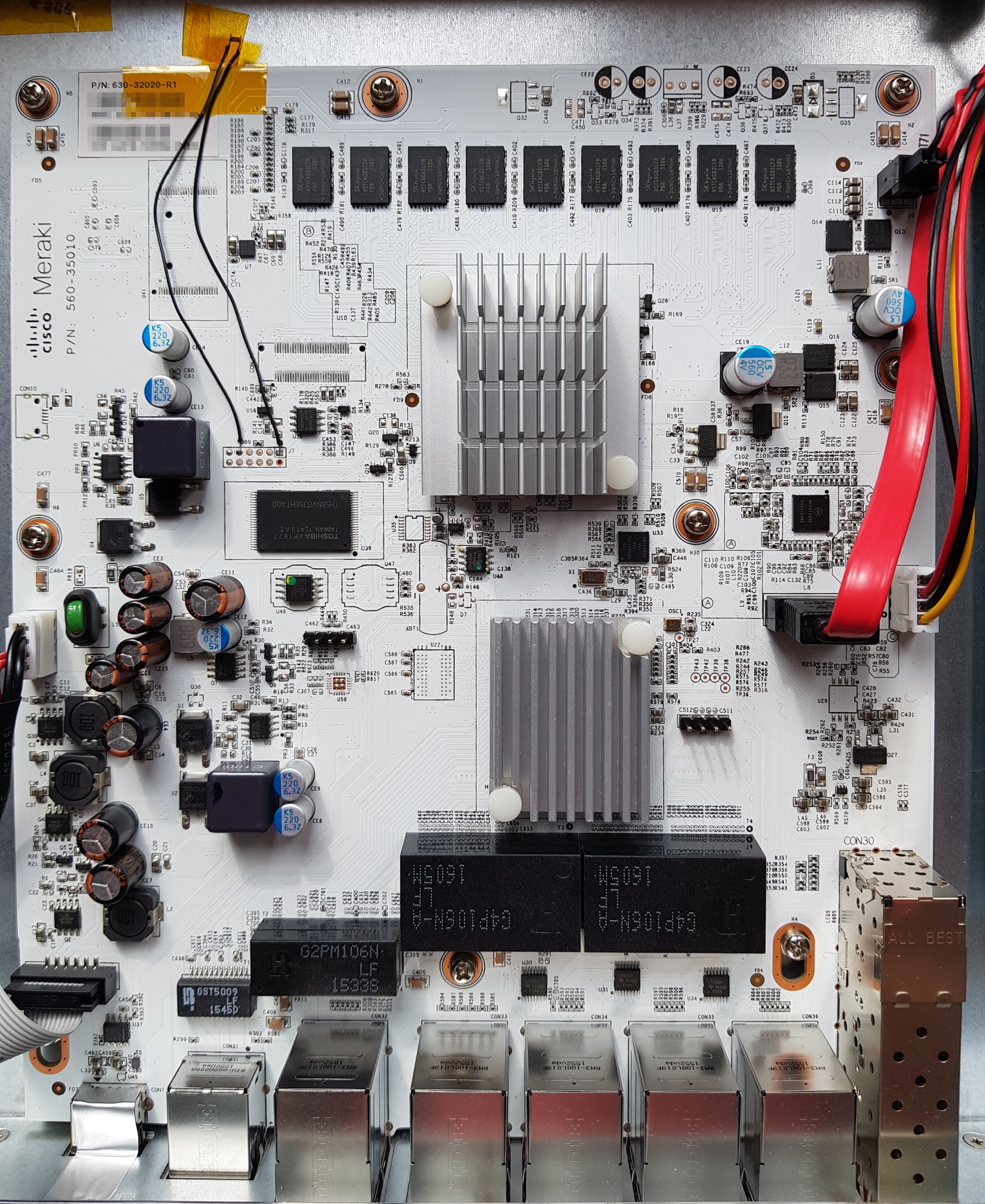
- Intel Atom C2358 CPU (2C/2T, 1.74GHz)
- 2GB DDR3 ECC RAM (SODIMM, Unigen U25U7210N8FD-BDD-CCHF1)
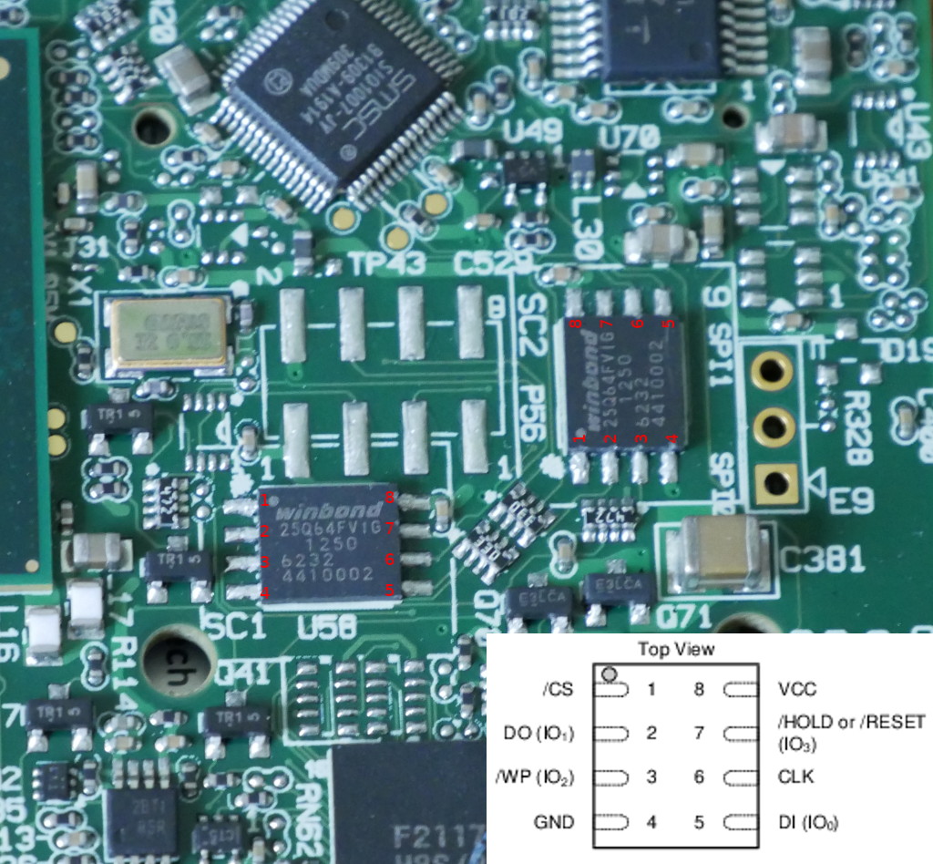
- 16MB SPI flash, 2GB NAND flash (TSOP48 NAND on motherboard, USB via Phison)
- MS350-24X: 30 Network interfaces (16 Gigabit Ethernet, 8 mGig Ethernet, 4 SFP+, 2 QSFP stacking)
- MS350-48: 54 Network interfaces (48 Gigabit Ethernet, 4 SFP+, 2 QSFP stacking)
- MS350-24X: MA-PWR-1025WAC
- MS350-48: MA-PWR-250WAC (identical to PWR-C2-250WAC)
The MS350 RAM can be upgraded: the 4GB (HMT351A7CFR8C) and 8GB (HMT41GA7MFR8C) PC3-12800E SODIMMs have been confirmed to work. Non-ECC SODIMMs are not compatible.
| Model | Codename | Part number |
|---|---|---|
| MS350-24 (P) | BigPony | 600-36010 (P: 600-36020) |
| MS350-48 (LP/FP) | BigPony | 600-36030 (LP: 600-36040, FP: 600-36050) |
| MS350-24X | Clydesdale | 600-48010 |
The MS350-48 uses the Broadcom BCM56547 (A0) ASIC, with BCM84740 PHYs. The MS350-24X uses the Broadcom BCM56546 (B0) ASIC, with BCM82578 and Aquantia AQR405 PHYs. PoE versions of the switch use the Broadcom BCM59121 PSE controller.
MS350-48:
00:00.0 Host bridge: Intel Corporation Atom processor C2000 SoC Transaction Router (rev 02)
00:01.0 PCI bridge: Intel Corporation Atom processor C2000 PCIe Root Port 1 (rev 02)
00:03.0 PCI bridge: Intel Corporation Atom processor C2000 PCIe Root Port 3 (rev 02)
00:0b.0 Co-processor: Intel Corporation Atom processor C2000 QAT (rev 02)
00:0e.0 Host bridge: Intel Corporation Atom processor C2000 RAS (rev 02)
00:0f.0 IOMMU: Intel Corporation Atom processor C2000 RCEC (rev 02)
00:13.0 System peripheral: Intel Corporation Atom processor C2000 SMBus 2.0 (rev 02)
00:14.0 Ethernet controller: Intel Corporation Ethernet Connection I354 (rev 03)
00:14.1 Ethernet controller: Intel Corporation Ethernet Connection I354 1.0 GbE Backplane (rev 03)
00:14.2 Ethernet controller: Intel Corporation Ethernet Connection I354 (rev 03)
00:14.3 Ethernet controller: Intel Corporation Ethernet Connection I354 (rev 03)
00:1f.0 ISA bridge: Intel Corporation Atom processor C2000 PCU (rev 02)
00:1f.3 SMBus: Intel Corporation Atom processor C2000 PCU SMBus (rev 02)
01:00.0 Ethernet controller: Broadcom Inc. and subsidiaries Device b547 (rev 01)
01:00.1 Ethernet controller: Broadcom Inc. and subsidiaries Device b547 (rev 01)
MS350-24X:
00:00.0 Host bridge: Intel Corporation Atom processor C2000 SoC Transaction Router (rev 02)
00:01.0 PCI bridge: Intel Corporation Atom processor C2000 PCIe Root Port 1 (rev 02)
00:03.0 PCI bridge: Intel Corporation Atom processor C2000 PCIe Root Port 3 (rev 02)
00:0b.0 Co-processor: Intel Corporation Atom processor C2000 QAT (rev 02)
00:0e.0 Host bridge: Intel Corporation Atom processor C2000 RAS (rev 02)
00:0f.0 IOMMU: Intel Corporation Atom processor C2000 RCEC (rev 02)
00:13.0 System peripheral: Intel Corporation Atom processor C2000 SMBus 2.0 (rev 02)
00:14.0 Ethernet controller: Intel Corporation Ethernet Connection I354 (rev 03)
00:14.1 Ethernet controller: Intel Corporation Ethernet Connection I354 1.0 GbE Backplane (rev 03)
00:14.2 Ethernet controller: Intel Corporation Ethernet Connection I354 1.0 GbE Backplane (rev 03)
00:14.3 Ethernet controller: Intel Corporation Ethernet Connection I354 1.0 GbE Backplane (rev 03)
00:1f.0 ISA bridge: Intel Corporation Atom processor C2000 PCU (rev 02)
00:1f.3 SMBus: Intel Corporation Atom processor C2000 PCU SMBus (rev 02)
01:00.0 Ethernet controller: Broadcom Inc. and subsidiaries Device b546 (rev 11)
Both models have the same USB devices present:
Bus 001 Device 002: ID 8087:07db
Bus 001 Device 001: ID 1d6b:0002
Bus 001 Device 003: ID 13fe:5200
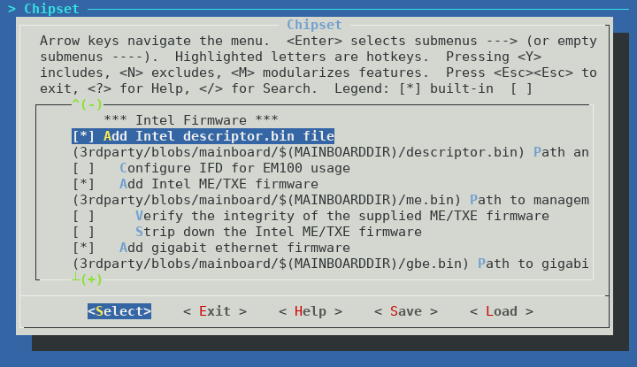
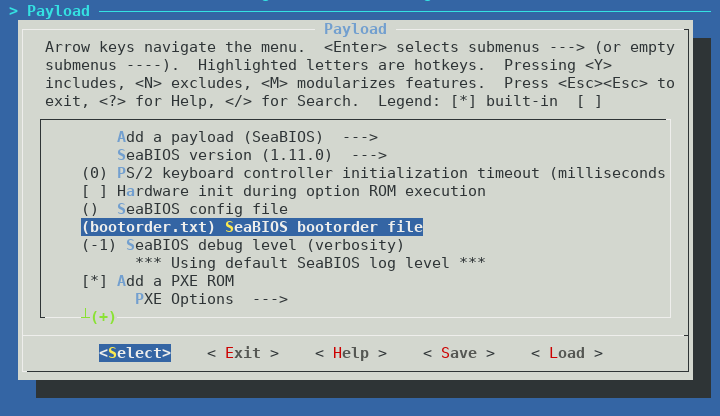
MS350-24X and MS350-48 both use coreboot as the bootloader, although the MS350-24X model has a different build. In both cases, the ROM has the following layout:
00000000:00010000 reserved
00010000:0070ffff bk1
00710000:00dfffff bk2
00e00000:00ffffff coreboot
The cbfs contains the following:
FMAP REGION: COREBOOT
ms350-24x_w25q128.bin: 16384 kB, bootblocksize 1024, romsize 16777216, offset 0xe10000
alignment: 64 bytes, architecture: x86

Name                           Offset     Type           Size   Comp
cmos_layout.bin                0xe10000   cmos_layout      1396 none
fallback/romstage              0xe105c0   (unknown)       21624 none
fallback/ramstage              0xe15a80   (unknown)       49421 none
fallback/payload               0xe21c00   simple elf      23042 none
config                         0xe27640   raw              4676 none
revision                       0xe288c0   raw               566 none
(empty)                        0xe28b40   null          1209432 none
mrc.cache                      0xf4ffc0   mrc_cache       65536 none
cpu_microcode_blob.bin         0xf60000   microcode       84992 none
(empty)                        0xf74c40   null            45912 none
fsp.bin                        0xf7ffc0   fsp            389120 none
(empty)                        0xfdf000   null           134040 none
coreboot was built with an ELF payload (miles) which by default loads and jumps into the bootkernel FIT image located at 0x10000. A secondary bootkernel exists on flash at offset 0x710000.
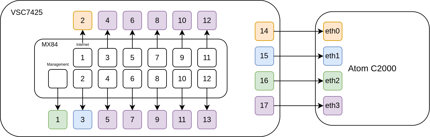
This is very similar to the MX84 as they are both based on the same Rangeley platform.
The entire MS350 series is based on the Intel Atom C2000 series CPU, which Meraki also used in the MX84. Sadly, the MS350 also suffers from the AVR54 errata, as the C2358 in both the MS350-48 and MS350-24X is the B0 revision.
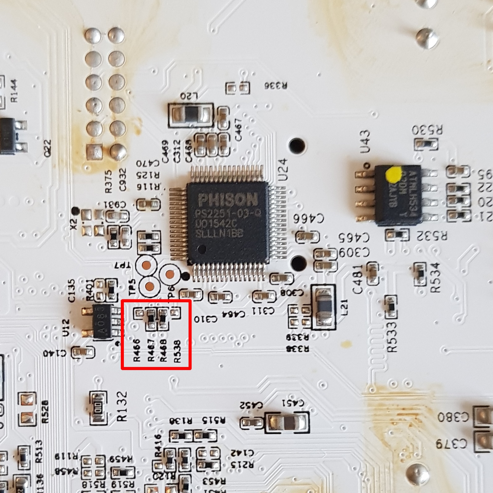
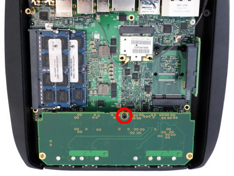
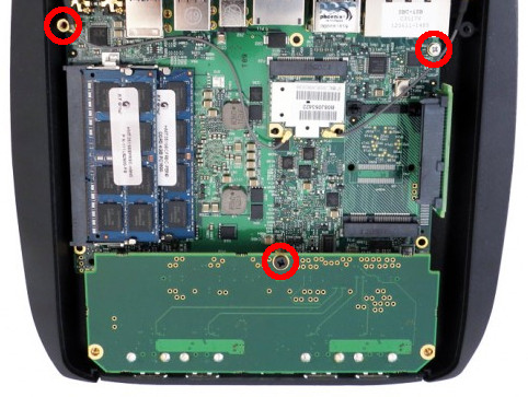
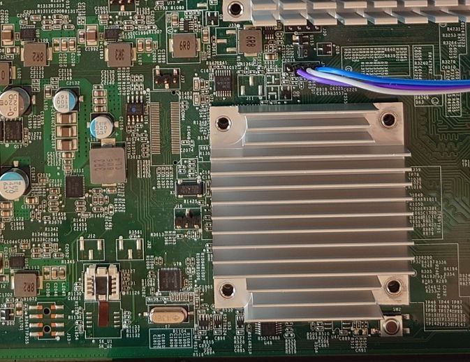
LPC_CLK is exposed on pin 1 of J35, with R3635 carrying 3.3V (MS350-48 and MS350-24X). Therefore, you can add a 100 Ohm resistor between R3635 and pin 1 to pull up the LPC clock. Just be sure to use an “extended-life” resistor for the modification, you wouldn’t want to compromise the MTBF of your Meraki product with anything sub-par 😉
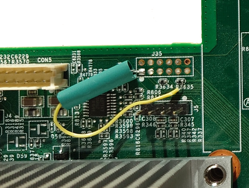
100 Ohm resistor to pull up LPC clock (MS350-24X)
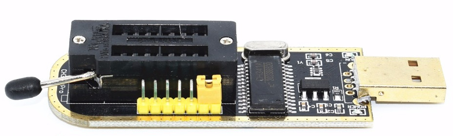
If you wish to flash your MS350, you will need to remove or socket the SOIC8 SPI flash (SK_U1).
This is because there are other devices powered by the +3.3V voltage rail used by SPI flash, which interferes with your ability to read/write the contents of flash. I prefer the Wieson G6179-10 SOIC8 socket (available from Adafruit). People outside the US will probably find it easier to desolder the flash and use a SOIC8 socket with prototype wires, as the G6179-10 is difficult to obtain for a reasonable price.
The UART header is J31 on both the MS350-48 and MS350-24X and follows the standard Meraki UART pinout (1: VCC, 2: Tx, 3: Rx, 4: GND)
Similar to the MS210/225 series, the Broadcom SDK implements the packet engine in userspace, using the linux_kernel_bde and linux_user_bde kernel modules to interface with the ASIC. In the Meraki firmware, the packet engine is a component of the userspace click daemon, which loads the bcm_click shared object during click router initialisation.
Idle power consumption:
- MS350-24: 45W
- MS350-24P: 57W
- MS350-48: 54W
- MS350-24X: 96W
GPL source code for the MS350 was requested from Meraki in July 2023. At the time of writing, they have not provided any. I will update this post with links to the source code when it is provided.