Tag Archives: meraki

Meraki MX84 overview

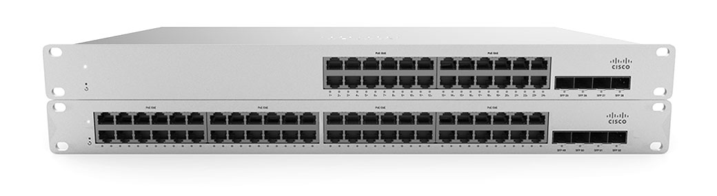
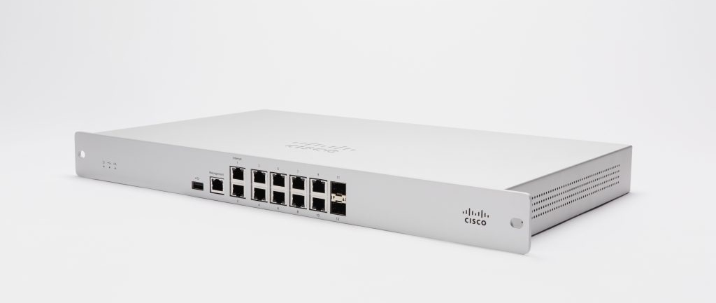
I became aware of the Meraki MX84 from Lathe Abusaid’s blog post about tearing down the hardware. After setting up an eBay alert and waiting, I finally won a job lot which included an MX84.


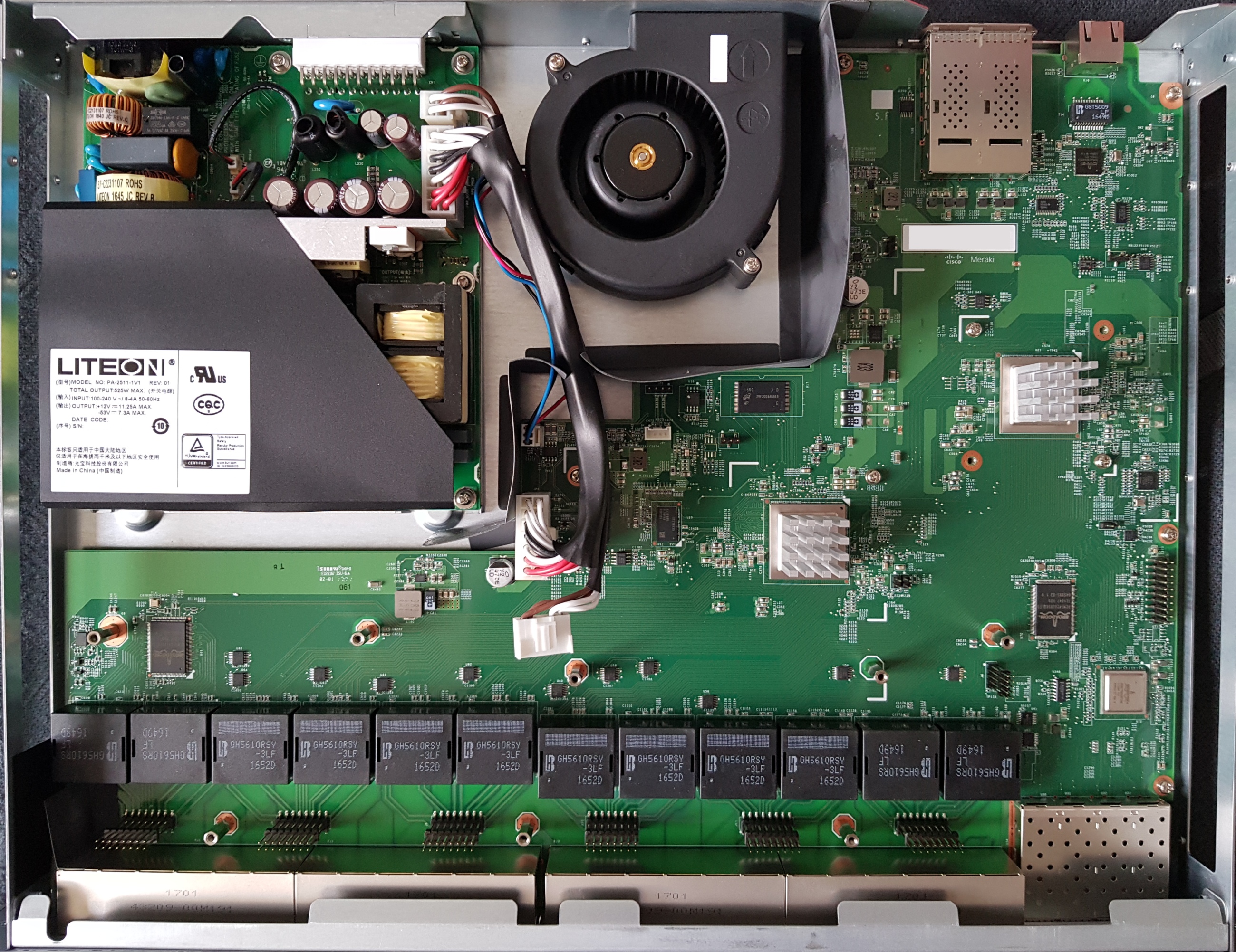
Here is a quick summary of the MX84 specs:

  • Intel Atom C2358 CPU (2C/2T, 1.74GHz)
  • 4GB DDR3 ECC RAM (H5TC4G83CFR-PBA)
  • Internal SATA port (1TB Western Digital Green)
  • External USB2.0 port
  • 13 Network interfaces (Vitesse VSC7425: 11 Gigabit Ethernet, 2 SFP)
  • 16MB SPI flash, 1GB NAND flash (Phison PS2251, USB on motherboard)
  • Fanless
  • Open frame 12V 2.5A power supply

The device runs Linux 3.18.131.

00:00.0 Host bridge: Intel Corporation Atom processor C2000 SoC Transaction Router (rev 02)
00:01.0 PCI bridge: Intel Corporation Atom processor C2000 PCIe Root Port 1 (rev 02)
00:03.0 PCI bridge: Intel Corporation Atom processor C2000 PCIe Root Port 3 (rev 02)
00:0b.0 Co-processor: Intel Corporation Atom processor C2000 QAT (rev 02)
00:0e.0 Host bridge: Intel Corporation Atom processor C2000 RAS (rev 02)
00:0f.0 IOMMU: Intel Corporation Atom processor C2000 RCEC (rev 02)
00:13.0 System peripheral: Intel Corporation Atom processor C2000 SMBus 2.0 (rev 02)
00:14.0 Ethernet controller: Intel Corporation Ethernet Connection I354 1.0 GbE Backplane (rev 03)
00:14.1 Ethernet controller: Intel Corporation Ethernet Connection I354 1.0 GbE Backplane (rev 03)
00:14.2 Ethernet controller: Intel Corporation Ethernet Connection I354 1.0 GbE Backplane (rev 03)
00:14.3 Ethernet controller: Intel Corporation Ethernet Connection I354 1.0 GbE Backplane (rev 03)
00:16.0 USB controller: Intel Corporation Atom processor C2000 USB Enhanced Host Controller (rev 02)
00:17.0 SATA controller: Intel Corporation Atom processor C2000 AHCI SATA2 Controller (rev 02)
00:18.0 SATA controller: Intel Corporation Atom processor C2000 AHCI SATA3 Controller (rev 02)
00:1f.0 ISA bridge: Intel Corporation Atom processor C2000 PCU (rev 02)
00:1f.3 SMBus: Intel Corporation Atom processor C2000 PCU SMBus (rev 02)

The MX84 uses coreboot as the bootloader (coreboot-af6fa06-dirty-Liteon_GRM1001_MFG_v4.0.0; bootlog) and the ROM has the following layout:

00000000:00010000 reserved
00010000:0070ffff bk1
00710000:00dfffff bk2
00e00000:00ffffff coreboot

The cbfs contains the following:

FMAP REGION: COREBOOT
mx84.bin: 16384 kB, bootblocksize 1024, romsize 16777216, offset 0xe00000
alignment: 64 bytes, architecture: x86

Name                           Offset     Type           Size   Comp
cmos_layout.bin                0xe00000   cmos_layout      1352 none
fallback/romstage              0xe00580   (unknown)       25820 none
fallback/ramstage              0xe06ac0   (unknown)       61965 none
fallback/payload               0xe15d40   simple elf      20349 none
config                         0xe1ad00   raw              4310 none
revision                       0xe1be00   raw               712 none
(empty)                        0xe1c100   null          1261208 none
mrc.cache                      0xf4ffc0   mrc_cache       65536 none
cpu_microcode_blob.bin         0xf60000   microcode       84992 none
(empty)                        0xf74c40   null            45912 none
fsp.bin                        0xf7ffc0   spd            389120 none
(empty)                        0xfdf000   null           134040 none

coreboot was built with an ELF payload (miles) which by default loads and jumps into the bootkernel FIT image (dts here) located at 0x10000. A secondary bootkernel exists on flash at offset 0x710000.


Let us revisit those Intel I354 interfaces. As a networking appliance, the MX84 has a lot of network interfaces.

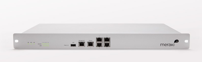
There are 13 network interfaces on the front (Management, Internet 1 & 2, Ethernet 3-10, and 2 SFP cages) so there should be a switch inside the MX84 or we would expect to see more than four interfaces in lspci.

In this case, the switch is the VSC7425, and even if you use the 3.18.131 kernel from Meraki, you won’t have any connectivity because all four of the I354 interfaces connect directly to the VSC7425

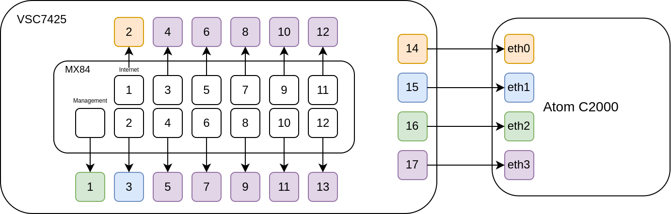
The stock Meraki firmware uses a binary called vtss_poca_d to initialise and configure the VSC7425, which does so using a proprietary Vitesse framework (PDF).

vtss_poca_d is a static binary, so could we use it with a newer kernel such as 5.10.146 found in OpenWrt 22.03?

$ vtss_poca_d
mdio_write16: SIOCSMIIREG on eth0 phy:0 reg:0 failed: Not supported
mdio_write16: SIOCSMIIREG on eth0 phy:0 reg:1 failed: Not supported
mdio_write16: SIOCSMIIREG on eth0 phy:0 reg:2 failed: Not supported
mdio_write16: SIOCSMIIREG on eth0 phy:0 reg:3 failed: Not supported
mdio_write16: SIOCSMIIREG on eth0 phy:0 reg:0 failed: Not supported
mdio_write16: SIOCSMIIREG on eth0 phy:0 reg:1 failed: Not supported
mdio_write16: SIOCSMIIREG on eth0 phy:0 reg:2 failed: Not supported
mdio_write16: SIOCSMIIREG on eth0 phy:0 reg:3 failed: Not supported
mdio_write16: SIOCSMIIREG on eth0 phy:0 reg:0 failed: Not supported
mdio_write16: SIOCSMIIREG on eth0 phy:0 reg:1 failed: Not supported
mdio_read16: SIOCGMIIREG on eth0 phy:0 reg:2 failed: Not supported
mdio_read16: SIOCGMIIREG on eth0 phy:0 reg:3 failed: Not supported
mdio_read16: SIOCGMIIREG on eth0 phy:0 reg:2 failed: Not supported
mdio_read16: SIOCGMIIREG on eth0 phy:0 reg:3 failed: Not supported

Nope! As such, it is very unlikely this device will ever be supported by OpenWrt.


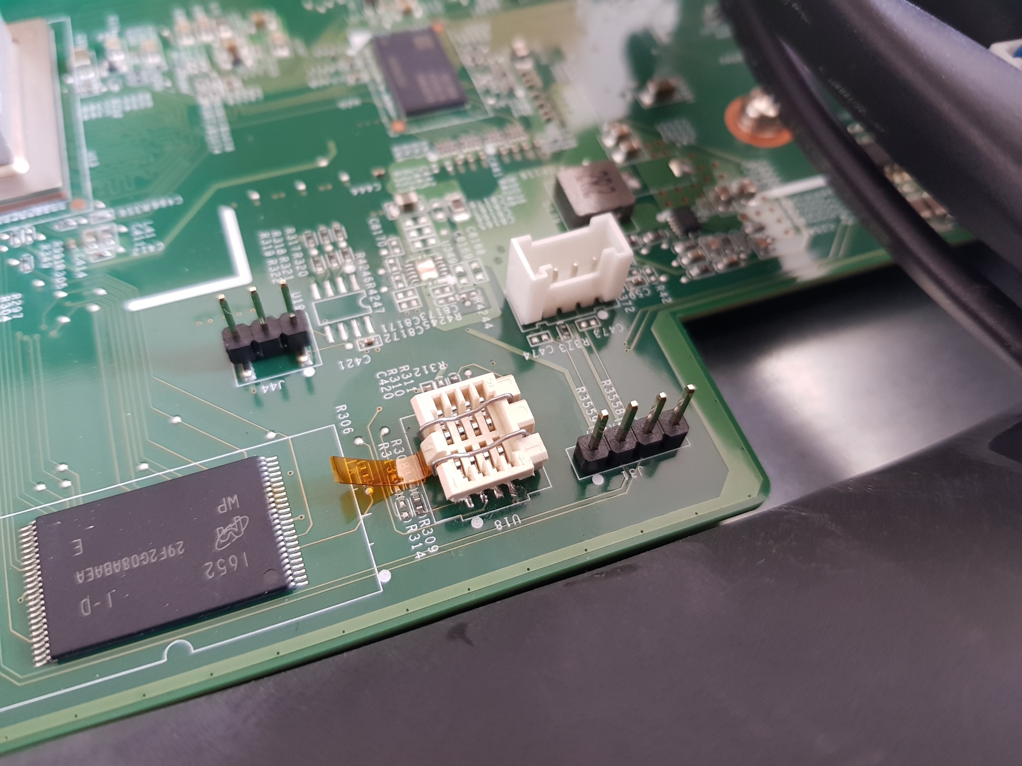
You may have noticed that the MX84 is based on the Atom C2000, a CPU which suffers from the AVR54 errata. When I first received my MX84, there was no output on UART and the power consumption was a suspiciously consistent 6W, all the hallmarks of a device dead from AVR54. There are numerous instructions for how to revive a Synology NAS with a dead Atom, but no such instructions exist for the MX84.

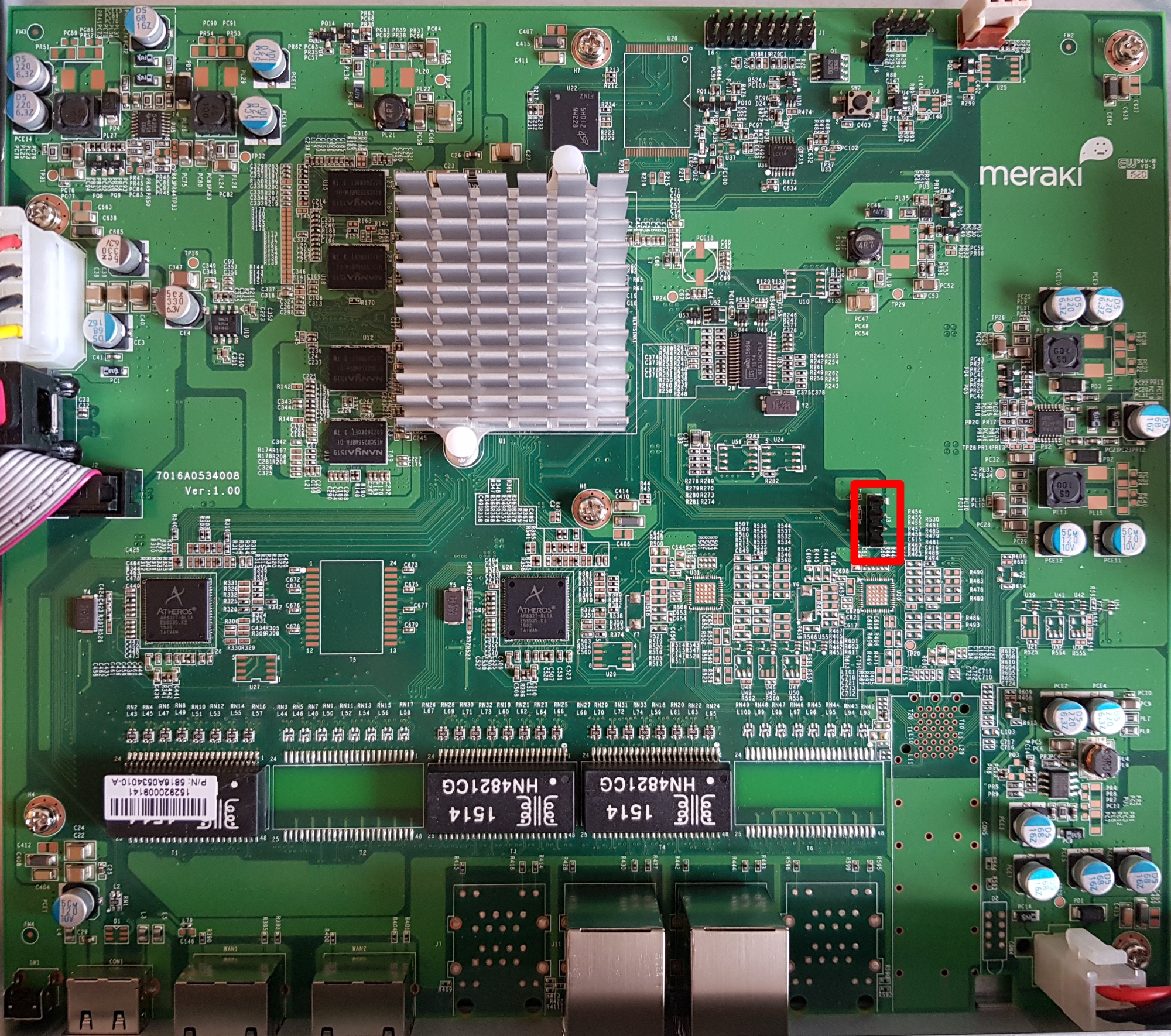
Fortunately for me, there was a photo from Lathe Abusaid’s blog post which provided a crucial hint. It appears that the MX84 unit photographed in their teardown includes a 100 Ohm resistor between pins 1 (LPC clock) and 9 (3.3V) of header J7.

This solution appears to have been chosen because it was the most convenient for Cisco, however note that pin 9 of J7 appears to be a GPIO output which, depending on the coreboot payload, may not always be active high. I would suggest instead soldering to pin 8 of the unpopulated SOIC8 nearby (U47), which will provide 3.3V regardless of the payload GPIO configuration.

That being said, here is a photo of the resistor fix to J7 that I just advised against doing, taken before realizing pin 9 was a GPIO

After soldering the pull-up resistor, the LPC clock is back on pin 1 of J7:

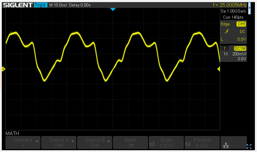
Oscilloscope output of the LPC clock on pin 1 of J7 after adding a 100Ω resistor


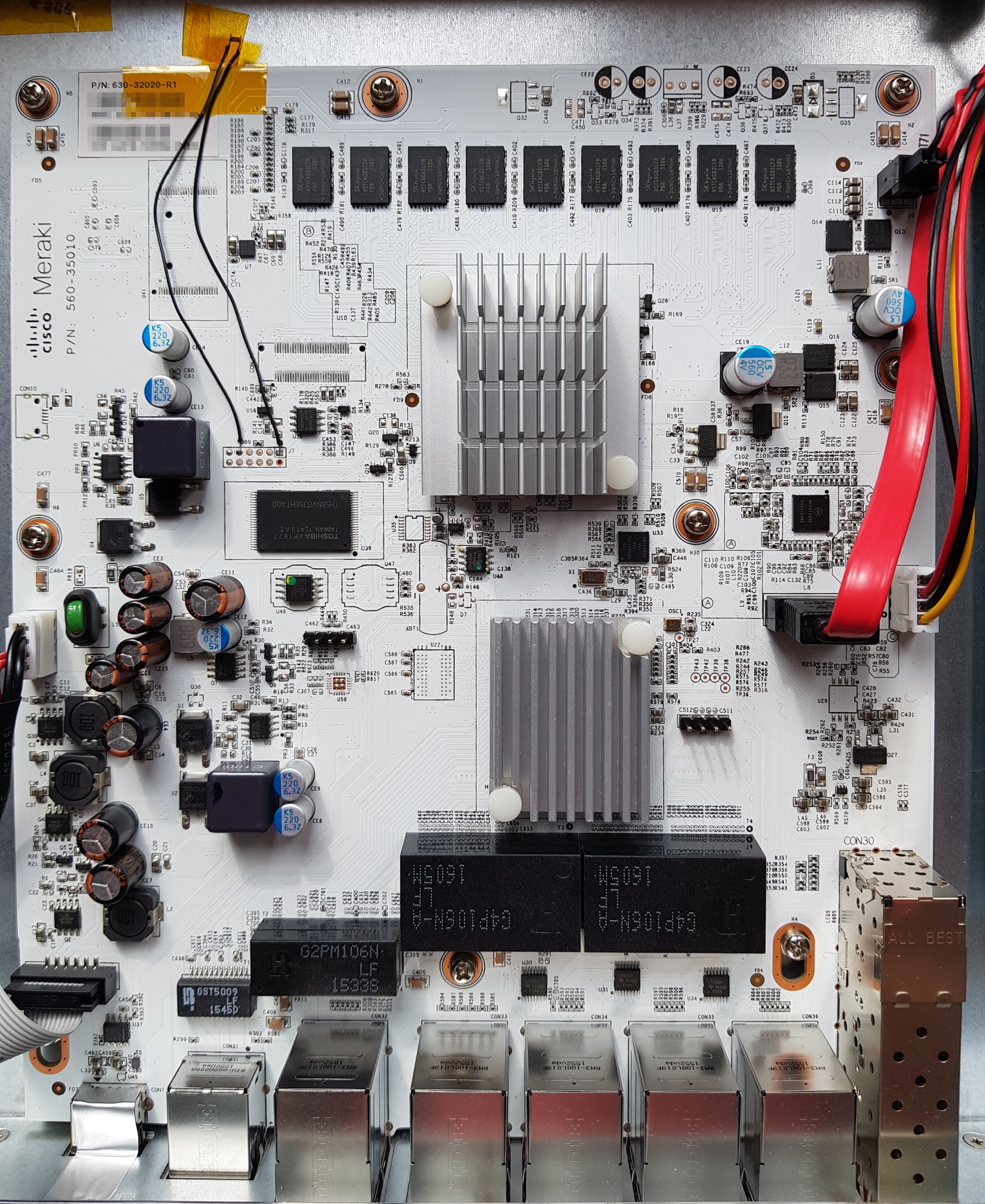
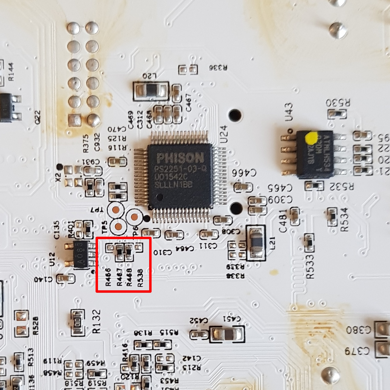
There is an unpopulated footprint for a Micro-USB port on the left side of the motherboard. By default the D-/D+ are not connected, as the 0 Ohm resistors are unpopulated (they are instead populated on R467/R468 connecting the Phison ps2303q to the Atom CPU). I believe this port was used during development to easily swap the USB drive connected to the SoC.


One question I had about the MX84 was: why coreboot? It seems that this design is based on Intel’s “Mohon Peak” reference platform. From the Intel customer reference board (CRB) documentation (PDF):

The embedded firmware ecosystem has developed an example boot loader solution
for the CRB that uses the FSP kit. This solution is based on the open source Coreboot
project at coreboot.org. While Intel does not endorse or support boot loader solutions
based on the Coreboot project, the example Coreboot-based boot loader provides a
good teaching model for how to integrate the Intel FSP into a complete boot loader
solution.

Now it is clear why Meraki chose to use coreboot, that is simply the bootloader reference provided by Intel for Mohon Peak. Other manufacturers who made Atom C2000 products also used coreboot (such as the VeloCloud 520-AC).

Meraki provided the coreboot source code in December 2022, after a delay of more than 12 months. The coreboot source code for the MX84 is available on GitHub.


Meraki hardware commanding the premium that it does, if you are considering buying an MX84: don’t. The VeloCloud 520-AC (C2358) and 540-AC (C2558) are available for ~$30 on eBay and have the C0 revision which doesn’t suffer from AVR54.

If you already own an MX84 and want to poke around, here is a buildroot based firmware that you flash to SPI. The firmware will boot, initialize the switch, DHCP, and start an SSH server (the root password is the device serial without hyphens). Note that it is initramfs based, so no changes are persisted.

Caveat emptor: VeloCloud devices have an issue with the igb/I354 compatibility, meaning that only the two SFP cages are functional. However, that is two more interfaces than you will get from the MX84 (zero) with any other kernel.

Meraki MS210/MS225 hardware overview

The Meraki MS210 and MS225 series switches offer 24 or 48 ports of Gigabit Ethernet, four SFP/SFP+ uplink ports, a dedicated remote management port, and stacking capabilities via QSFP.

Meraki MS210-24 and MS210-48


Here is a quick summary of the MS210/MS225/MS250 specs:

  • Broadcom Broadcom BCM56160 “Hurricane3” ASIC
  • Broadcom BCM82756 10G PHY
  • Broadcom BCM59121 PSE controller (PoE models only)
  • 16MB of SPI flash (MX25L12805D)
  • 1024MB DDR4 RAM (soldered)
  • 256MB of NAND (MT29F2G08ABAEAWP)
MS225-48LP internal PCB

MS225-48LP switch internals with PoE midplane removed


The Meraki codename for the MS210, MS225, and MS250 series is “brumby” and all brumby switches run the same firmware release (switch-arm). The MS250 is essentially the MS225 with hot-swap power supplies (similar to the MS220/MS320).

Keen readers may be wondering why the MS210 series has only SFP ports while the MS225 has SFP+ ports, given they are identical hardware and run the same switch-arm firmware. The answer is market segmentation; Meraki decided to artificially limit the speed of the MS210 SFP ports to 1G, even though the MS210 hardware is capable of 10G via SFP+. Early in the boot process switch_brain checks the switch model, and if it identifies as the MS210 series the SFP port speed is limited to 1000M.

The stock Meraki boot process uses u-boot on SPI to load a “bootkernel” (also from SPI), which then initializes NAND and using kexec boots the main firmware. The firmware layout follows the standard Meraki practice of having A/B firmware images: bootkernel1, bootkernel2, part.safe, part.old.


If you wish to flash your MS210/MS225, you will need to remove or socket the SOIC8 SPI flash (U18). This is because the ASIC is powered by the same +3.3V voltage rail as the SPI flash, and will attempt to boot when you attach your flashing device, which interferes with your ability to read/write the contents of flash. I prefer the Wieson G6179-10 SOIC8 socket (available from Adafruit). People outside the US will probably find it easier to desolder the flash and use a SOIC8 socket with prototype wires, as the G6179-10 is difficult to obtain for a reasonable price.

MS225 with SPI flash socket installed

Unlike the MS120, the MS210/MS225 do not implement secure boot, so all that is needed to develop on the platform is to recompile and flash u-boot from the Meraki GPL release and then interrupt the boot process and provide your own firmware build (e.g. via TFTP).

The UART header is J31 on both the 24 and 48 port models and follows the standard Meraki UART pinout (1: VCC/3.3V, 2: Tx, 3: Rx, 4: GND) at 115200 baud.


The Broadcom SDK for the BCM56160 series implements the packet engine in userspace, using the linux_kernel_bde and linux_user_bde kernel modules to interface with the ASIC. In the Meraki firmware, the packet engine is a component of the userspace click daemon, which loads the bcm_click shared object during click router initialisation.

There are no public datasheets available for any of the Broadcom chips used in the MS210/225. While you can find information on OpenBCM, as far as I can tell the API provided by OpenBCM (via the kernel modules) which is used to implement the packet engine has no public documentation. If anyone has more information, please get in touch 😀


Model Meraki Board Part number
MS210-24 (P) BRUMBY_24 600-58015 (P: 600-58025)
MS210-48 (LP/FP) BRUMBY_48 600-58035 (LP: 600-58045, FP: 600-58055)
MS225-24 (P) BRUMBY_24 600-58010 (P: 600-58020)
MS225-48 (LP/FP) BRUMBY_48 600-58030 (LP: 600-58040, FP: 600-58000)
MS250-24 (P) BRUMBY_24 600-58050 (P: 600-58060)
MS250-48 (LP/FP) BRUMBY_48 600-58070 (LP: 600-58080, FP: 600-58090)

Meraki MX80: buildroot firmware

Ten years ago, before ARM was in everything, many embedded systems that did not justify using an x86 used PowerPC (or MIPS). This leads us to today’s subject: the Meraki MX80, an “enterprise security appliance.”

Meraki MX80 marketing image

Meraki MX80

The MX80 is End-of-Life (EOL) and can be purchased quite inexpensively on eBay.

The MX-series differs from other Meraki networking products of the 2010-era that we have previously covered (the MS220) in that it is PowerPC based (APM86290) with 2GB of RAM and 1GB of NAND flash. The factory bootlog of the device can be found in this GitHub gist.


MX80 PCB with uart header highlighted

MX80 UART header

Removing the cover allows you to connect to the UART header J3 (57600n8), with the pinout:

  1. VCC (don’t connect)
  2. Rx
  3. Tx
  4. GND

Ground (pin 4) is closest to the Ethernet ports.

Obtaining a root shell is very easy as u-boot has a 1 second boot delay and accepts input on UART. The default meraki_boot target sets the bootargs from meraki_bootargs which appends extra_bootargs, so just override rdinit with /bin/sh to prevent the Meraki OS from booting.

setenv extra_bootargs rdinit=/bin/sh
run meraki_boot

Once the MX80 has booted, bring up eth0 (port label Internet on the MX80):

$ mount -t proc proc /proc
$ mount -t sysfs sysfs /sys
$ ifconfig lo up
$ ifconfig eth0 up
$ udhcpc eth0

Once you have functional networking, you can dump the contents of NAND to a remote host for further analysis:

$ cat /proc/mtd
dev:    size   erasesize  name
mtd0: 00100000 00020000 "firmware"
mtd1: 00100000 00020000 "environment"
mtd2: 00040000 00020000 "oops-old"
mtd3: 3fdc0000 00020000 "ubi"
mtd4: 40000000 00020000 "all"
mtd5: 0201d800 0001f800 "part1"
mtd6: 0201d800 0001f800 "part2"
mtd7: 0001f800 0001f800 "board-config"
mtd8: 2001f000 0001f800 "storage"
$ dd if=/dev/mtdblock4 bs=1M | gzip -c | nc -l -p 5000

Running binwalk on “part1” shows us the structure of Meraki’s firmware:

$ binwalk part1.bin

DECIMAL       HEXADECIMAL     DESCRIPTION
--------------------------------------------------------------------------------
1024          0x400           device tree image (dtb)
16384         0x4000          device tree image (dtb)
131072        0x20000         uImage header, header size: 64 bytes, header CRC: 0xD84034B5, created: 2020-05-29 01:15:36, image size: 2447726 bytes, Data Address: 0x0, Entry Point: 0x0, data CRC: 0xCE3A4A5E, OS: Linux, CPU: PowerPC, image type: OS Kernel Image, compression type: gzip, image name: "Linux-3.4.113"
131136        0x20040         gzip compressed data, maximum compression, from Unix, last modified: 1970-01-01 00:00:00 (null date)
4194304       0x400000        uImage header, header size: 64 bytes, header CRC: 0xDA83B155, created: 2020-05-29 01:16:17, image size: 16719915 bytes, Data Address: 0x0, Entry Point: 0x0, data CRC: 0x2381914F, OS: Linux, CPU: PowerPC, image type: RAMDisk Image, compression type: lzma, image name: "Simple Ramdisk Image"
4194368       0x400040        LZMA compressed data, properties: 0x5D, dictionary size: 67108864 bytes, uncompressed size: -1 bytes

There is a device tree image at offset 0x400 which seems to be for the MX60 (codename bluestone). There is a second device tree image at offset 0x4000 for the MX80 (codename fullerene).

It is not as simple as creating a binary image with the DTB at offset 0x4000, the kernel at 0x200000, and initrd at 0x40000 because Meraki have modified u-boot to have a custom command meraki which reads a header, verifies the contents of the ubi partition part1 or part2 with SHA1, and then sets environment variables from addresses defined in the header.

The layout of the header is as follows:

Header field Data type (value)
SHA1_MAGIC uint32 (0x8e73ed8a)
HEADER_LEN int32
DATA_LEN int32
SHA1SUM char[20]
MERAKI_EXTRA_MAGIC uint32 (0xa1f0beef)
MERAKI_EXTRA_LEN uint16 (0x0006)
MERAKI_EXTRA_TYPE uint16 (0x0001)
IMAGE_OFFSET uint32 (0x20000)
RAMDISK_OFFSET uint32 (0x400000)
FDT_OFFSETS array uint32 (0x400 or 0x4000)

The FDT used to boot depends on the value of meraki_part_fdt_index in u-boot. For the MX80, the index of the FDT offset is 1, meaning the FDT located at 0x4000 is used to boot. The presence of two FDTs suggests that Meraki are using the same firmware for both the MX60 and MX80. Despite the MX80 being a dual core CPU only one CPU core is usable, there is no SMP support in the kernel provided by Meraki.


To simplify booting, I have written a post-image.sh script which generates the appropriate header and assembles a bootable firmware image as part of the buildroot build process. You can find instructions on how to build the firmware in the meraki-builder GitHub repository.

The 3.4 kernel provided by Meraki doesn’t have any of the features required by OpenWrt (e.g. overlayfs) and buildroot doesn’t have a package manager. If you just want something to boot and run SSH on, then the buildroot image fulfills that need. You will most probably want to customize buildroot to include the packages and configuration that suits your needs. Upstream support in OpenWrt is still a long way away, as the APM86290 does not have support in the mainline kernel.